


Ref: z2615196m
Traditionally, discussions regarding field-programmable gate arrays (FPGAs) used in interfacing applications within communication systems have focused on raw I/O speed. Unfortunately, how an FPGA handles high-speed data once 'on chip' is commonly overlooked. Many FPGA architectures are ill equipped to handle this flood of data, which results in a bottleneck of large proportions. Ultimately, this bottleneck forces the designer to consider expensive work-arounds that exist when using traditional FPGAs pushing the performance envelope. For FPGAs to be considered viable solutions for next-generation, high-speed communications applications, a new FPGA architecture is required that is optimised to address and eliminate this bottleneck.
The bottleneck
Increasing bandwidth in the network and the explosion of communications standards and interfaces has created a troubling problem for traditional FPGA architectures. Until recently, the speed of the internal logic core of most FPGAs has kept up with system performance. However, with performance requirements for communications systems increasing dramatically, FPGAs are often unable to process data through the chip at wireline speeds.
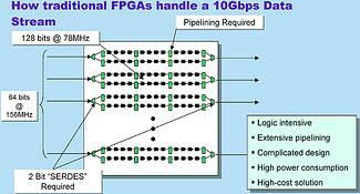
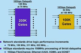
So, what are the options for a designer needing to handle a 10 Gbps Ethernet datastream? As an example, most ASSPs on the market today addressing 10 Gbps Ethernet will present using the XGMII interface standard (data at 64 bits wide operating at 156 MHz). This forces the designer using traditional FPGAs to use heavy pipelining and redundant logic to achieve the required system throughput. The bit width of the data must be doubled to 128 bits, once on chip so that operating frequency can be halved to 78 MHz. The result? A longer, more difficult design process, high power consumption and higher costs.
There are five areas in which the requirements for a new FPGA internal core architecture can be grouped - logic module, logic module cluster, embedded memory blocks, clocking schemes and routing structures.
Logic module
A high-performance core architecture needs a flexible logic module with minimal delay, but what about granularity? Fine granularity of two inputs allows minimal module delays and eases the burden on synthesis and mapping, but taxes the routing structure to the point of impracticality, creating excessive routing delays. Course granularity of seven or more inputs, while minimising routing delays, increases the burden on synthesis and mapping and creates greater module delays and inefficient logic utilisation for most datapaths. The optimal granularity appears to be in the range of 3-5 inputs, offering the best balance between flexibility and tool burden on one hand and logic efficiency and minimised delay on the other.
Logic module cluster
Nearly all FPGA architectures organise logic modules into clusters. A high-performance architecture requires a fully fracturable logic module cluster, meaning each logic module can be used independently of other modules within the same cluster and can be combined with any other logic module in the core. This architectural improvement enables greater levels of efficiency and higher logic module utilisation rates. A fully fracturable logic module also allows the placer greater flexibility, which decreases the distance between logic modules and results in better system performance.
At best, traditional FPGA architectures support only partial fracturability of the logic cluster, which often necessitates remapping before placement. This remapping can have an adverse impact on performance. In addition, the placer now has more restrictions regarding where certain functions of a given datapath can be placed, causing greater routing delays than expected.
Embedded memory blocks
Clearly, high-performance FPGA architectures require high-speed memory blocks, but attention needs to be paid to how memory is used in communication systems. When moving data from place to place, memory blocks often need to take the form of FIFOs. The best way to construct high-speed FIFOs is to build the control logic into the memory block. Adding an embedded FIFO controller results in higher speeds and increased logic efficiency as no internal logic is needed to construct the control logic, as with traditional FPGA architectures. In addition, the embedded controller eliminates the concern that a FIFO controller built out of soft gates would compete with the designer's logic for device resources or system performance.
Additionally, since designers of high-performance communication systems have to contend with multiple clock and phase domains, the embedded control logic should allow for asynchronous reads and writes as well as prevent metastability conditions, providing the designer the ability to easily cross clock and phase domains.
Clocking scheme
Modern communications designs require a flexible clocking scheme that is fairly transparent to the user and does not add to the design task. All global clocks should be available equally to all sequential resources on the chip, thereby eliminating the need for clock floorplanning. Quadrant-clocking schemes found in traditional FPGA architectures place an additional burden on the placer and could cause areas of congestion on the chip, thereby degrading system performance.
Additional enhancements to the clocking structure can further reduce the burden on the placer and help eliminate bottlenecks. For example, the architecture should allow the global clocks to be sourced from different resources: package pins, internal PLLs or even internal logic. Another improvement would be a segmentable clock structure, allowing for a high number of local, higher frequency clocks. Finally, the architecture should allow for additional clock networks to be constructed out of general routing resources for maximum flexibility.
Routing structure
Often the routing scheme of an FPGA architecture is overlooked, but, in fact, it is the single most important aspect of any PLD architecture. Because the routing scheme works in conjunction with the other elements of the architecture (logic modules, logic module clusters, embedded memory and clocking scheme) to achieve the required system performance, it takes on an even more important role when constructing a high-performance FPGA internal core architecture. The routing structure determines how efficient the architecture is and ultimately determines the maximum performance possible.
Of course, the speed of the interconnect element is important, but size also plays a role. The smaller the better as a smaller element allows for an abundant interconnect. Abundant interconnect allows the router to routinely achieve close to the theoretical Manhattan Rule wire length between logic modules, and therefore minimal delays. Critical to a high-speed architecture is a programmable interconnect element that does not take up valuable substrate real estate, such as SRAM-based interconnect, allowing for shorter distances between logic modules.
The routing scheme should be non-hierarchical - logic modules should be able to access high-speed routing tracks without having to go through short-distance resources first. This non-hierarchical routing scheme should provide the router with more than one type of routing resource that can be used to connect any two logic modules. Also, the routing structure should consist of high-speed local tracks, segmented local tracks of varying lengths, as well as across-chip routing tracks. And lastly, the routing scheme should also work in conjunction with dedicated routing buffers to speed up high fanout nets.
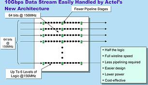
Increasing bandwidth in the network and the explosion of communications standards and interfaces has created a troubling problem for traditional FPGA architectures. Until recently, however, the speed of the internal logic core of most FPGAs has kept up with system performance. However, with performance requirements for communications systems increasing dramatically, FPGAs are often unable to process data through the chip at wireline speeds (ie, 64 bits at 156 MHz). Therefore, to eliminate this bottleneck, a new high-performance FPGA architecture is required to handle the high data rates. This new architecture should have the following specifications: a logic module with moderate granularity (3-5 inputs) to balance the load between synthesis, mapping and placement; A fully fracturable logic module cluster to allow the placer more options and enable high logic module utilisation; Embedded memory blocks with built in FIFO control to ease the construction of the high-performance FIFOs required for communication systems and minimise the use of vital internal resources; a flexible clock scheme that obviates the need for clock floorplanning and allows for multiple clock sourcing schemes; a high-performance routing scheme that allows the placer to achieve close to theoretical Manhattan Rule wire lengths between logic modules.
The AX architecture
Actel's recently announced AX architecture begins to address these issues. The AX architecture provides a high-speed, high-performance platform which when used in communications applications can enable money, power and time savings. Axcelerator, the first FPGA family based on AX relieves the communications bottleneck by providing 500+ MHz internal performance, high-speed embedded FIFOs and a high-speed clocking infrastructure. The future will see the introduction of BridgeFPGA products based on AX which will not only eliminate the communications bottleneck but will further enhance communications systems with the inclusion of embedded protocol controllers.
For more information contact ASIC Design Services, Kobus van Rooyen, 011 315 8316, [email protected]
| Tel: | +27 11 315 8316 |
| Email: | [email protected] |
| www: | www.asic.co.za |
| Articles: | More information and articles about ASIC Design Services |


© Technews Publishing (Pty) Ltd | All Rights Reserved
 printer friendly version