


Ref: z2708351m
FPGAs have proven to be a valuable technology in today's electronic industry, offering performance, time-to-market, and cost advantages. Evidence of their pervasiveness is the fact that almost every printed circuit board (PCB) now contains at least one FPGA. But, does the process of putting the FPGA on a PCB compromise those highly valued benefits? This paper examines the move from ASIC to FPGA technology, and the impact of FPGA on board integration today.
The promise
There is a reason that so many companies are turning from ASIC to FPGA design: FPGAs today support multimillion gate, high-performance design. From a business perspective, a migration from ASIC to FPGA technology allows an opportunity to:
* Reduce capital risk (eliminate ASIC non-recurring expense).
* Minimise ASIC development capital risk (FPGA as prototype).
* Reduce time to market (no ASIC production cycle).
* Maintain competitive flexibility late into the design cycle (easy to change the design).
* Maximise total product ROI (use FPGA for product introduction, roll over to ASIC to reduce product component costs).
* Open new markets (product volume and price point will not support ASIC implementation).
* Explore new manufacturing and assembly efficiencies (the physical FPGA devices are not design-specific).
* Enhance product quality (FPGAs are 100% tested at the device level).
* Upgrade products in the field (provide customers with new features and defect correction programming).
Without detailing all of the business benefits associated with leveraging FPGA technology in the product development process it should still be quite clear that FPGAs are not simply a technology. They represent a discontinuous event that will transform business models. Corporations that are able to accurately describe the true relationship between FPGA technologies and their business models will gain a significant competitive advantage while obtaining new operation efficiencies and capital liquidity.
The reality
From a business point of view, FPGA design sounds too good to be true. It is. Unless corporations are strictly developing standalone chips or using FPGAs as an ASIC prototyping platform, the FPGA is placed on a PCB. Once one or more FPGAs are part of the PCB, the cost benefit that FPGAs alone provide, can quickly be lost. Why?
Multimillion gate FPGAs are typically designed by teams. Teams also design complex PCBs. In many corporations these teams are in independent arms of the engineering organisation. In some cases, the design teams are geographically dispersed. It is common that these two teams do not communicate well because the issues and methodology of designing within a chip differ from those of designing within the context of a PCB.
Within minutes an FPGA designer may completely reconfigure the FPGA device interface to the PCB. Those few minutes may cause catastrophic changes to the PCB physical design, sometimes requiring the PCB designer to start over.
While Figure 1 is a tremendous oversimplification, it does focus attention on the interaction between the FPGA and PCB design processes and teams as the primary opportunity for increased efficiencies. In simple terms, the FPGA design process must interface well with the PCB design process. FPGA changes must be communicated to the PCB design, be evaluated within the PCB design context, and then any necessary changes must be communicated back to the FPGA design process, to achieve product requirement convergence.
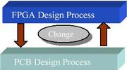
The interactions between the FPGA and PCB design processes are typically manual. Information is generated in the FPGA design process and fed into the PCB design process though e-mail, spreadsheet, or document. Then, the PCB design team must manually create a matching description of the FPGA for use in the PCB logical and physical design tools. Changes to the FPGA may result in changes to the logical design of the PCB but more frequently result in substantial changes to the PCB physical design. The changes are incorporated and the system design is furthered analysed.
Estimating the cost of integration
Determining the actual integration costs requires a product-by-product exploration. One approach is to identify every element of the integration process that costs time and money and then form a mathematical model. This allows you to perform 'what if' analysis to understand the true integration cost. Actual numerical data from past or present projects can be used to validate the model.
Suppose that a company decides that the total cost of integrating FPGAs on PCBs is based on four main factors:
CTotal = CFPGAPCB + CFPGA UpdatePCB + CPCBRe-spin + COpportunityProduct
Where:
* CFPGAPCB is initial cost to create the logical symbol of the FPGA for the PCB schematic and to create the physical symbol & associated data.
* CFPGA UpdatePCB is cost to update the changed FPGA interface in the PCB logical and physical designs.
* CPCBRe-spin is cost to re-spin PCB prototype due to errors, interfaces out of date, or system timing issues.
* COpportunityProduct is cost of the lost sales due to not having the product available to sell
The next step is to determine the constituent parts of each of the four main costs.
For the initial cost (CFPGAPCB) one common method is to measure the impact on cost based on the number of FPGA pins that change. So, this variable could be defined by:
CFPGAPCB = RPCBCost * ((NFPGA PinsProduct/PSymbolCreation) + (NFPGA PinsProduct/PPackageCreation) + TFPGAPCB)
Where:
* RPCBCost hourly wage of the PCB resource.
* NFPGA PinsProduct total number of FPGA pins in the product.
* PSymbolCreation symbol creation productivity measured in number of pins per hour.
* NFPGA PinsProduct package creation productivity measured in number of pins per hour.
* TFPGAPCB time required to connect the FPGA symbol to the PCB schematic measured in pins per hour.
Building on the theme of using FPGA pin count as a cost measure, the variable for changing the FPGA interface (CFPGA UpdatePCB) could be defined by:
CFPGA UpdatePCB = NFPGA InterfaceChanges * (RPCBcost * ((XFPGA PinsProduct/PSymbolUpdate) + (XFPGA PinsProduct/PPackageUpdate) + TUpdate FPGAPCB logical + TUpdate FPGAPCB physical))
Where:
* NFPGA InterfaceChanges number of times the FPGA interface changes over the complete product design process.
* RPCBcost hourly wage of the PCB resource.
* XFPGA PinsProduct number of pins changing per interface change iteration.
* PSymbolUpdate symbol update productivity measured in number of pins per hour.
* PPackageUpdate package update productivity measured in number of pins per hour.
* TUpdate FPGAPCB logical time required to update the FPGA design on the PCB schematic side.
* TUpdate FPGAPCB physical time required to drive the FPGA changes into the PCB physical layout, measured in pins per hour.
At this point, a company could measure the cost of initial integration and the cost of an FPGA change (no re-spins and no lost opportunity costs). Using the cost of an engineer at $50 per hour and one change to an interface results in a linear curve showing cost per pin change:
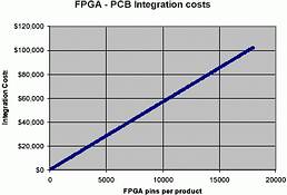
Holding all variables constant and only increasing the number of iterations shows the escalating cost of change. For example, at 20 interface changes and 10 000 FPGA pins in the design, the cost is over $200 000.
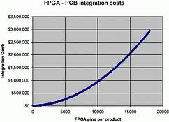
The company can define and establish the cost of a re-spin (CPCBRe-spin) in order to add that effect to the cost equation. For example, the company determines the re-spin cost is $5000 per spin. Holding CFPGAPCB + CFPGA UpdatePCB constant, and using 100 for the number of interface changes and a value for the number of pins changing per re-spin of 1000, results in the following graph:
Lastly, adding in the cost of lost opportunity to the equation, the total integration cost is realised. For example, the company holds the values of CFPGAPCB + CFPGA UpdatePCB constant and retains the value of one re-spin at $5000. If it takes three days for the re-spin, and the company establishes that the lost opportunity cost is $10 000 per day the following graph results:
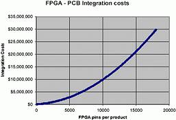
By using a simple, four element cost equation, the company can predict the impact of FPGA integration based on pin changes. This impact can easily approach the cost of ASIC design.
Returning the benefits
The key to returning the benefits that FPGA designs promise is to try to reduce as many of the variables in the cost equation to zero. This is the focus of the Mentor Graphics FPGA on Board initiative:
* Connectivity closure: automatically create the FPGA symbol for the PCB and manage any interface changes between the FPGA and PCB design processes.
* Timing closure: automate the changes to the interface due to meeting timing constraints and manage updates between the FPGA and PCB design processes.
Mentor Graphics chose to start with automating connectivity closure. Today, one can use FPGA Advantage to design the FPGA and through BoardLink, and can automatically generate the PCB symbol in minutes and place it in the PCB schematic using DesignView. In addition, connectivity changes are managed.
Conclusion
Every company in the business of creating electronic designs has the information available to realise the benefits of FPGA design. After a company makes the decision to integrate FPGAs into their PCB design, they will encounter FPGA to PCB integration issues. These issues will only increase as FPGA capacity and performance increases.
Corporations that learn to effectively deploy FPGA technology in their product development process, accounting for and minimising integration costs, will be able to bring products to market faster and with a higher profit margin than their competition.
| Tel: | +27 11 315 8316 |
| Email: | [email protected] |
| www: | www.asic.co.za |
| Articles: | More information and articles about ASIC Design Services |


© Technews Publishing (Pty) Ltd | All Rights Reserved
 printer friendly version