


Designing printed circuit boards in today's electronic industry presents unique challenges. To help manage all the complex requirements that make up circuit board design, EDA software must be both powerful and flexible.
One design phase where tool flexibility is particularly critical is plane generation, where power and reliability are needed to support numerous net assignments and unique component connection requirements.
When evaluating PCB layout tools, one capability to look for is the flexibility to generate multiple plane types. With PowerPCB, you get powerful plane-generation tools that make it easy to create copper planes, copper pour planes, and split/mixed-planes. This document provides an overview of each plane type and the benefits each brings to the design community. The technique chosen for any given design will depend on the designer's requirements.
Copper planes
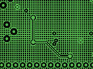
Generally, designers choose to generate plane layers with standard copper data when they need to cover specific design areas that do not require electrical intelligence. Those areas can have copper data in the form of rectangular areas, round areas, custom polygonal areas with any number of corners, or paths (paths represent lines, not closed polygons). Controlled by a series of settings, these polygons can be filled or hatched, depending on the default values you assign to line width and hatch grid at the time of creation (Figures 1 and 2).
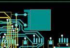

To generate custom plane patterns, PowerPCB allows you to vary the look of the plane areas by altering their shapes with user-defined settings, or by building intersecting patterns of copper data. To equalise their potential and avoid creating spacing errors during the verification process, copper areas can be assigned a consistent signal name.
Copper areas can be placed on any electrical layer, in any size, and in any location. They can also be easily modified to accommodate changes that occur during the design cycle. By assigning net names to polygons, copper planes can easily be assigned to any element of a signal (eg, pads, vias, traces) on the board.
Copper-pour planes
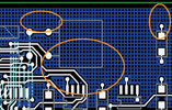
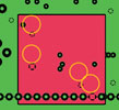
Copper-pour planes consist of polygons with associated electrical intelligence. This intelligence enables copper pours to automatically fill design areas such that they maintain clearances from other electrical objects in the area being filled. With PowerPCB, objects like text, routes, pads and vias can all be cleared automatically without difficulty (Figure 3).
Copper-pour planes are generated as easily as copper planes. Simply draw a polygon on a particular layer in the area that needs to be poured, assign a net, and flood it. Also, like copper plane areas, copper-pour planes can be defined as rectangular, round, or polygonal shapes, with their fill data being controlled by varying the hatch grid and default line width assigned during plane generation.
By assigning net names to copper-pour planes, you can connect electrical items directly to them. PowerPCB adds thermals automatically wherever the planes share the same signal name as the electrical objects (Figure 4).

One big advantage that copper-pour planes have over copper planes is that copper pours automatically clear objects that do not contain the same signal name. This creates a smooth clearance distance around the circuitry within the pour area. This distance is sometimes referred to as 'trace shielding', since it helps reduce the amount of trace susceptibility on highspeed/sensitive nets.
PowerPCB uses assigned electrical design constraints to determine how far away the pour data should be from other electrical items in the area. These constraints, which are easily assigned upfront with DxDesigner or ePlanner, can be at a variety of levels, including net, class, and group (Figure 5). This allows copper pours to be multidimensional. PowerPCB makes it easy to manage clearance sizes for items (such as pads, vias, and traces on a particular net) within the area that may need larger clearances than the same type of item on all other nets.
To differentiate copper-pour polygons from other poured polygons in the same design or on the same layer, you can vary the settings (eg, via status, polygon width, hatch direction) to create unique patterns for each polygon (Figure 6). This degree of flexibility is essential for today's complex design requirements.
Split/mixed plane generation
Split/mixed planes are yet another type of plane generation supported by PowerPCB. This feature enables you to create both the copper-pour polygons described above, plus more.
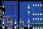
With split/mixed planes, you can bury traces on inner plane layers quickly, easily, and with great accuracy (Figure 7). The electrical awareness of copper pours allows automatic clearing of electrical information embedded within the plane layers. Split/mixed planes also enable you to generate split planes quickly and flawlessly.
Plane layer thermal assignments can be a difficult task with today's ever-changing complex designs. With the introduction of low-voltage ICs, designers find themselves having to complete internal multiple-voltage planes (mixed powerplane layers), a task that is made easier and more seamless when sufficient visual aids are readily available.
To support multiple voltages on power planes, you must be able to identify pads/vias and isolate them into their respective planes - a task that is difficult to do with negative image planes. Visualisation is the best way to separate planes. With the 'View Nets' feature in PowerPCB, you can assign unique colours to connections and/or pads, making it easy to identify which pads are assigned to specific nets, to locate pads on specific voltage nets, and to separate the complex plane with a single construction line.
Custom thermal definitions add additional flexibility to support the unique requirements of today's difficult split-power/ground-plane layers. With PowerPCB, via definition provides the ability to create an unlimited number of via types and assign custom thermal requirements to them (Figure 8). Designers can then assign the desired via to a net so that only that via will be included in route data. When the split-plane layers are generated, the defined thermal type for pads and vias will be added automatically, thus enabling the proper plane connections to be created.
Conclusion
Plane generation is just one of the areas in which PowerPCB excels, helping designers to do their jobs better and faster. The feature-rich design environment and intuitive GUI of PowerPCB make it an unsurpassed design station capable of addressing today's complex PCB layout problems quickly, easily, and affordably.
| Tel: | +27 11 315 8316 |
| Email: | [email protected] |
| www: | www.asic.co.za |
| Articles: | More information and articles about ASIC Design Services |


© Technews Publishing (Pty) Ltd | All Rights Reserved
 printer friendly version