


Ref: z2801165m
In the fiercely competitive GSM phone terminal market, terminal manufacturers have come to expect solutions that expedite their development and cycle times. This, coupled with the new feature-rich handsets with mega-pixel cameras, Bluetooth technology and multimedia functions, designers are demanding smaller and more integrated high-performing modules that consume less board space.
In order to meet the increasingly complex phone terminal designs, component solutions providers are challenged to meet ease of use requirements while providing enhanced performance. Micro Devices' designers have met the challenge with the RF3166 quad-band GSM/GPRS power amplifier (PA) module.
The RF3166 is RFMD's latest third-generation PowerStar PA module with patented integrated power control and is designed to maximise transmitter yields and minimise design time. The integrated power control function eliminates the need for directional couplers, detector diodes, power control ASICs and other power control circuitry, which allows the module to be driven directly from the DAC output. Integrated power control also enables higher levels of integration, reduced cost and enhanced performance. The benefit of this technology is single-point calibration in all four bands enabling manufacturers to achieve simple and efficient phone calibration during production.
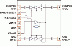
The high-power, high-efficiency RF3166 PA module is self-contained with 50 Ω input and output terminals. The device is designed for use as the final RF amplifier in GSM850, EGSM900, DCS and PCS handheld digital cellular equipment and other applications in the 824 MHz to 849 MHz, 880 MHz to 915 MHz, 1710 MHz to 1785 MHz and 1850 MHz to 1910 MHz bands. On-board power control provides over 50 dB of control range with an analog voltage input and power down with low logic for standby operation.
Designers derive three key benefits with the RF3166:
1. An improved layout versus previous generations, with the PA requiring no external components or critical routing.
2. Technology improvement: VBATT tracking circuit (VBATT = battery voltage).
3. Optimal tuning performance.
Physical implementation improvements
The RF3166 is the market's first true 6 x 6 x 1,4 mm (36 mm²) quad-band GSM power amplifier module because it requires no external bypass components and no critical routing. All of the RF matching and bypassing is performed on the low-cost substrate construction of the RF3166. RFMD engineers have taken care to design the I/Os in such a way that radio board designers do not have to cross over RF lines in order to match up to the device. Compared with previous generation modules, requirements for external pin-to-pin routing of collector voltages have been eliminated. The external routing of signals is straightforward and simple. This realises a compact layout, with minimal keep-out areas to ensure the smallest possible TX solutions. For the first time with the RF3166, layout and small size come together in a high-performing solution in a small footprint.
Technology improvement: VBATT tracking circuit
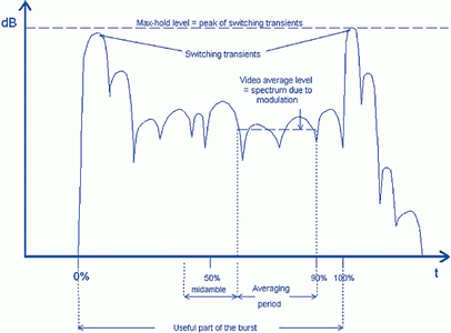
One issue that challenges phone designers is meeting performance parameters over extreme conditions. It is especially difficult to meet system transient spectrum requirements during low battery conditions. Figure 3 illustrates that the up-ramp and down-ramp of the GSM burst have the greatest influence on transient spectrum. In order to minimise switching transients, ramping waveforms should be as smooth as possible, preferably sinusoidal. Any sharp transitions introduce high harmonic content, thus increasing transient levels. This problem is exacerbated when VBATT is close to VCC, which occurs during low battery conditions.
Automatic VBATT tracking circuit
The RF3166 incorporates a VBATT tracking circuit, which monitors battery voltage and automatically adjusts VRAMP in order to prevent the power control loop from reaching saturation. Without VBATT tracking, the VRAMP voltage must be adjusted in software in order to meet output RF spectrum (transient) requirements during low voltage battery conditions. This places the burden on phone designers to detect and compensate for VBATT changes in software. The addition of VBATT tracking circuitry alleviates this burden and ensures robust performance over more operating conditions.
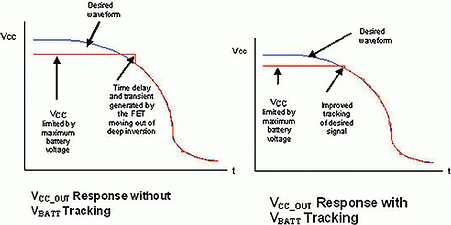
The VBATT circuit works by sensing the onset of stored charges and limiting the VRAMP voltage to prevent excess charges from building up. Excess charge storage causes saturation, which affects the response time of the MOSFET. During saturation, there will be a delay in the power control circuit following the VRAMP input, until the charge is transferred. This causes a lag in the circuit and a step in the resulting control voltage to the PA.
Figure 4 illustrates the sharp transition in the control voltage to the PA, which causes increased transients. By preventing VCC from becoming too close to VBATT, the magnitude of transients can be significantly reduced. This function is fully integrated into the CMOS controller and requires no additional inputs from the user. The user inputs the standard VRAMP signal and the controller automatically adjusts VRAMP when it is required. A block diagram of this integrated feature of the RF3166 architecture is shown Figure 5.
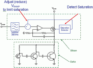
When VRAMP approaches VBATT, a saturation detector outputs a correction signal that limits the VRAMP signal to the integrator. The correction signal is subtracted from the VRAMP input signal, reducing the VRAMP so that VCC is sufficiently below VBATT.
During normal operation, when VBATT >> VCC, the saturation detector will not output any correction signal. The saturation detector will only output a correction (VRAMP reduction) in the case where VCC ~ VBATT. Generally, this will only happen when the handset battery is running flat.
An additional benefit of the VBATT tracking circuitry is that the usable VRAMP range can be extended. Without the VBATT tracking circuit, some designers will preset the VRAMP voltage based on the lowest possible battery voltage condition in the handset, resulting in reduced output power and efficiency. With VBATT tracking, VRAMP can be set to its maximum value for nominal battery conditions, thus allowing the designer to access the full VRAMP range and gain back any output power and efficiency deficiencies.
An example of the effectiveness of the VBATT tracking circuit is shown in Table 1.
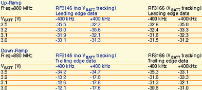
VBATT tracking example
Table 1 shows ±400 kHz transient TX spectrum data for both a standard RF3146 and the new RF3166, which includes the VBATT tracking circuit. The data is presented for both up-ramp (leading edge) and down-ramp (trailing edge) transients. The standard RF3146 features the first generation CMOS controller while the RF3166 integrates the new controller with VBATT tracking.
Table 1 shows that the transient spectrum at nominal (+3,5 V) or high VBATT values is optimal for both controllers. However, as the VBATT voltage drops we see a corresponding decrease in transient response, particularly on the RF3146. The RF3166 transient spectrum also decreases, but it maintains a transient spectrum well within the system requirements.
It should be noted that the RF3146 meets transient spectrum when VRAMP is reduced manually. The VBATT tracking circuit alleviates developers from that responsibility by automatically making the adjustment.
Additional circuitry has been incorporated into the RF3166 to filter some of the noise and spurious signals derived from the baseband DACs. This filter allows handset designers to have better noise margin in system design, thereby simplifying design efforts.
Optimal tuning performance
With the RF3166, RFMD designers have achieved a high degree of power and current flatness over all four bands. This makes for a device that is easier to optimise and tune for the best current consumption. Designers can also implement robust transmit solutions quickly and take advantage of superior efficiency.
An ideal world would consist of RF components with 50 Ω terminal impedance, and cellphone designers would simply bolt components together in the smallest space possible. However, in the real world, not only does impedance deviate from 50 Ω, it also varies with frequency.
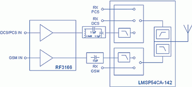
An example that illustrates this concept is the complexity of matching a PA module to an antenna switch module (ASM) module that is not a 50 Ω component. To enable the PA and the ASM to meet customer requirements, calls for broadband matching circuits.
By using the power contours and impedance levels presented by the RF3166, a matching circuit derived from standard RF practices yields a well-behaved, robust TX solution.
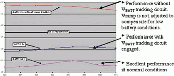
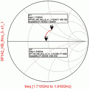
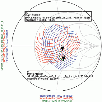
Figure 8 shows a block diagram of the application board with matching circuits. The matching circuits include a simple series capacitor for the GSM band and a three-element high pass network for the DCS/PCS bands. Figure 9 overlays the RF3166 power contours with the actual impedance response of the DCS/PCS matching network plus industry standard ASM. RFMD took advantage of the variation in ASM impedance to track the power contours in order to achieve power flatness while optimising efficiency.
By choice and optimisation of the interface matching circuits, the designer has flexibility to meet target performance objectives. The following example demonstrates typical results that can be achieved on evaluation boards by using intelligent matching techniques.
In our example, the goals are to design a matching circuit and TX solution that is:
* Triple-band operation (GSM900, DCS, PCS).
* Max GSM Pout @ Antenna = 33,5 dBm.
* Max DCS/PCS PMout @ Antenna = 30,5 dBm.
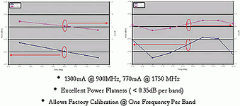
* Power flatness within 0,5 dB per band.
* All harmonics <-40 dBm.
With only a few components, the phone board layout can be realised quickly. In this case excellent power flatness was achieved, and the applications engineers used a judicious matching circuit design to minimise current consumption.
It is interesting to see why a 50 Ω match is not always preferred. When comparison data is taken between the example and the RF3166 designed for 50 Ω operation, one can see that some significant tradeoffs occur.
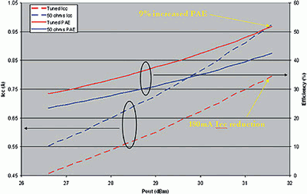
In this test, we compared a standard evaluation board (50 Ω) vs the evaluation board tuned for optimal efficiency. For the 50 Ω case, we assumed a 1,6 dB post-PA loss to achieve 30 dBm at the antenna (31,6 dBm out of PA). It should be noted that a higher VRAMP was afforded the optimal tuned board because we were able to tune for the optimum Pout. In this case VRAMP = 1,636 for tuned board versus VRAMP = 1,471 for the 50 Ω evaluation board. Recall that the VBATT tracking circuit allows phone designers to operate the PA with a higher VRAMP voltage without having to worry about switching transients for low battery conditions. This is the key to achieving improved efficiency performance.
The results were striking. We achieved a 9% efficiency improvement at 31,6 dBm (30 dBm at antenna) for the optimally-tuned board relative to the 50 Ω board. It also showed 180 mA current reduction at 31,6 dBm. This underscores the rationale for optimally tuning the RF3166 performance to meet overall systems goals. Looking at the 50 Ω data exclusively does not tell the true performance one can expect when designing with actual components.
Summary
The third-generation RF3166 PowerStar PA module builds upon the key features of previous generations of RFMD's PowerStar solutions with integrated power control and adds improved layout benefits, VBATT tracking enhancements and flexibility for optimum performance.
| Tel: | +27 21 555 8400 |
| Email: | [email protected] |
| www: | www.rfdesign.co.za |
| Articles: | More information and articles about RF Design |


© Technews Publishing (Pty) Ltd | All Rights Reserved
 printer friendly version