


Introduction
Printed circuit boards (PCBs) are getting more complex, dense and difficult to manufacture as more functionality and features are included into every piece of electronic equipment. This is necessary to differentiate, gain and maintain a competitive edge. For years, PCB designers had little concern over the fabrication analysis aspect of bare PCBs; that was left to bare board suppliers. In addition, most of the EDA tools for PCBs lacked the sophisticated rule and checking routines necessary to perform a thorough fabrication analysis of bare boards.
The need for analysis
What does this have to do with designers of PCBs and fabrication analysis? All along, PCB engineers needed to finish each project faster, free of errors, easy to manufacture, test and repair. For this task designers employed sophisticated EDA tools to design PCBs and verify correctness based on electrical design rules specified by engineering. But these checks did little to verify for manufacturability, and traditional EDA design software had limited checks for fabrication defects.
Once the PCB design was finished, the engineer and/or designer would create Gerber files and send them 'over the wall' to the fabricator. In many cases, PCB designers know the manufacturing steps required to build a bare PCB board, but they are generally unaware of advances in manufacturing, new materials or technologies that affect how their designs are built. This necessitates investment in educating PCB designers in the area of bare board manufacturing and 'best design practices.' More importantly, PCB designers must be empowered to perform manufacturing checks themselves.
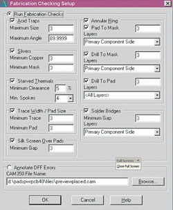
After completing a design, the designer usually outputs Gerber files and sends them to the fabricator. The fabrication facility performs an analysis to ensure there are no errors and the design meets their fabrication processes, including:
* Acid traps - corners where etchant could potentially be trapped, compromising electrical connectivity.
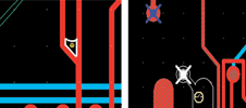
* Solder/paste mask slivers - small pieces of the solder mask or solder paste material that 'break' off.
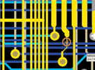
* Starved thermals - undersized copper traces insufficient to carry voltage/current from power/ground plane to device.

* Min trace width/pad size - sufficient to ensure highest yield, voltage/current carrying capability.
* Silkscreen over pads - ink could flow into via hole compromising electrical integrity.
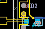
* Annular ring checks - check for sufficient clearance to power/ground planes.
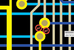
* Solder bridges - potential for short.
If the fabricator finds any manufacturing errors, they are fixed. But did they notify the designer that there were errors? If so, the process of correcting the original design is typically manual and error prone. If not, any future iterations of that design would contain the same errors, requiring the same fix at the fabricators over again. The better PCB fabricators will notify the designer about errors, but the fabrication software tools that they use most likely are not compatible with the EDA board design software. This results in manual, error-prone methods of passing information (paper, e-mail, etc) to correctly fix these problem areas. Introduction of such human interpretation is the greatest cause of errors in designs. Further, fixing errors may introduce new fabrication errors and we are back at square one again.
Conclusion
The ability to check for fabrication problems within the EDA PCB design software environment solves a number of problems and yields many benefits. First, and most importantly, it removes the dependency on the fabricator to catch errors late in the design cycle. Future redesigns will not perpetuate the same fabrication problems. In addition, moving the fabrication of bare boards from the prototype facility to mass production (in many cases, a different supplier) eliminates the dependency on a different fabricator to find the same errors, since they were not involved earlier in the design phase. This will best ensure prevention of manufacturing stops due to errors encountered, with the added benefit of waiving NRA charges when designers perform these checks within their working environment ahead of time.
The better EDA vendors of PCB design software understand the importance of advanced prefabrication analysis and provide this important capability to board designers.
About the author: Yan Killy has over 20 years of experience in PWB design for switching power supplies and analog and digital equipment. He possesses extensive knowledge of mechanical fastening for electronic assemblies, bare board fabrication and testing, in addition to comprehensive knowledge of UL, CSA and TUV/VDE safety requirements.
| Tel: | +27 11 315 8316 |
| Email: | [email protected] |
| www: | www.asic.co.za |
| Articles: | More information and articles about ASIC Design Services |


© Technews Publishing (Pty) Ltd | All Rights Reserved
 printer friendly version