


Freescale Semiconductor has won the race to be the first company to commercialise magnetoresistive randomaccess memory or MRAM. The first commercial device to use the MRAM technology is its standalone 4 Mbit MR2A16A integrated circuit, which Freescale announced on 10 July 2006.
This memory technology, which uses magnetic moments to store the bit state, has been fully-qualified for use in commercial tier applications. There are many unique features of the MR2A16A that can open up interesting market opportunities for this device.
MRAM features
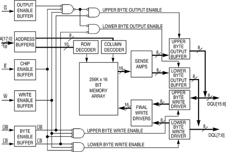
The 4 Mb MR2A16A is arranged in a 256K x 16-bit configuration. It is an asynchronous design that uses standard chip enable, write enable, and output enable pins that allow system flexibility and prevents bus contention. Separate byte enable pins allow flexible data bus control where data can be written and read as 8 bits or 16 bits. MRAM is inherently a non-volatile memory technology that can retain its memory contents for a minimum of 10 years without the need for power.
The MR2A16A has infinite write-cycling capability. Empirical studies have shown the MR2A16A bit cells to endure over 58 trillion write and read cycles under the worst case operating conditions. To date, no endurance failures have been recorded with the MR2A16A bit cell and the bit cycling study is ongoing.
The MR2A16A is fabricated using the 0,18 μm process technology along with a proprietary MRAM process technology used to create the bit cell. A total of five layers of interconnect is formed out of both technologies. The chip runs on a 3,3 V supply. It has symmetrical high-speed write and read access times of 35 ns. The device also allows for fully static operations.
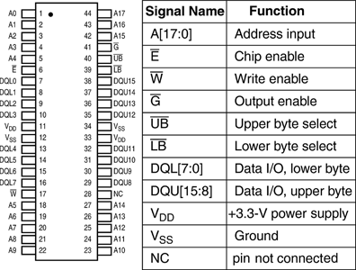
This first MRAM device is available in a 44-pin TSOP type-II package with RoHS compliance. It is configured with an industry-standard centre power and ground SRAM pinout so that it can be used in existing hardware that uses the same SRAM configuration in its application. (See Figures 1 and 2.)
MRAM applications
At this time, the MR2A16A is most valuable in commercial applications where it is imperative to save data during a system crash. When a system undergoes a power failure, there are critical data parameters that need to be saved quickly before all power is lost. The data parameters stored in the MR2A16A can later be retrieved to diagnose or debug issues that caused the system failure to occur. The device is a great solution for this type of 'black box' application because it is able to write data at SRAM speeds before total power loss occurs, while being able to retain the data once all power is gone.
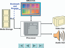
MRAM is also well-suited for entertainment applications that have resume play features. During power down, bookmarks that indicate the timestamp of the media that was played are quickly stored on the non-volatile MRAM memory. A subsequent power up and resume play can then be performed almost instantaneously (see Figure 3).
Security systems can benefit from MRAM by managing encryption. Encryption parameters can be stored quickly and be retained during system shutdown. Likewise, gaming machines require fast data parameter storage and data integrity during a power loss.
Bit cell operation
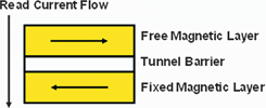
The MR2A16A has toggle bit cells that contain one transistor and one magnetic tunnel junction (1T1MTJ). The magnetic tunnel junction or MTJ is at the heart of the MRAM bit cell. It is comprised of a very thin aluminium oxide (Alox) - chemical name: Al2O3 - dielectric layer placed between two magnetic layers. Each of the magnetic layers has a magnetic polarity associated with it. The top magnetic layer is called the free layer because it has the freedom to flip polarities. The bottom magnetic layer is called the fixed layer because the polarity is locked and does not change.
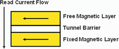
It is the polarity of the free layer that determines whether a bit is programmed to a '0' state or a '1' state. When the polarity of the free layer and the polarity of the fixed layer are aligned (pointing in the same direction), the resistance through the MTJ stack is low (see Figure 4). When the polarity of the free layer and the fixed layer are opposed by 180° (pointing in the opposite direction), the resistance through the MTJ stack is high (see Figure 5). It is this low and high resistance through the MTJ stack that determines whether a bit cell is read as a '0' or a '1'.
During the programming operation, the polarity of the free layer is toggled to one of two directions. The polarity is set with copper interconnects running in perpendicular directions on the top and bottom of the MTJ. A dose of current across the perpendicular interconnects creates a magnetic field which toggles the polarity of the free layer in the opposite direction (Figure 6).
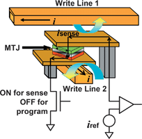
One major drawback to productising MRAM as a reliable memory, is the high bit disturb rate. When the target bit is being programmed, the free layer in an untargeted bit can be programmed inadvertently. Freescale researchers have overcome this issue by creating a toggle bit cell that rotates the magnetic moment in the same direction each time the state of the bit is flipped. A staggered pulse of current on write line 1 and write line 2 rotates the polarity without disturbing bits along the same row or column as the target bit.
To further isolate untargeted bits from being disturbed, Freescale has surrounded the copper interconnects with a layer of cladding on three sides of the copper. This cladding directs and focuses the strength of the magnetic field toward the target bit cell. This allows the target bits to be programmed using a much lower current and isolates neighbouring bits from the magnetic field that would normally induce a disturb.
Another difficulty in mass producing an MRAM device is due to the extremely thin Alox tunnel barrier. Small thickness variations in the Alox will produce large differences in the bit cell resistance. Freescale has solved the issue of the Alox variation to produce uniform tunnel barriers across the memory array, across the wafer surface and across production lots.
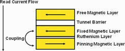
Freescale has also modified the fixed magnetic layer approach by adding two additional layers. Below the fixed layer is a Ruthenium (Ru) layer. And below the Ru layer is another magnetic layer called the pinning layer. The polarities of the fixed layer and the pinning layer oppose one another which will cause a strong coupling effect. This coupling allows the polarity of the fixed layer to stay locked so that it does not inadvertently flip with the application of the magnetic field used during the programming operation (Figure 7).
Advantages over other memories
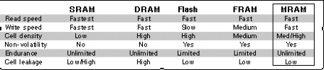
MRAM has many distinct advantages over other types of memories (see Table 1).
* Flash: Flash technology uses a charge stored on a piece of floating polysilicon (floating gate) laid over a gate oxide. The programming of a Flash bit cell requires a high voltage field that accelerates electrons fast enough so that the electrons can overcome the energy barrier of the oxide between the silicon and the floating gate. This causes the electrons to punch through the oxide and charge the floating gate which alters the threshold voltage of the bit cell transistor. Repeated transfers of electrons through the oxide causes a gradual wear out of the oxide material so that the Flash memory is limited to only 10K-1M write cycles before the bit is no longer functional. With continuous writes, some Flash memory can wear out as quickly as 10 days. MRAM, on the other hand, is able to endure an infinite number of write cycles because there is no charging or discharging involved. Magnetic polarities are rotated during programming which is a non-destructive and non-degrading operation.
During programming, Flash requires a high voltage to draw the electrons through the oxide material. MRAM uses current to create a magnetic field to program the free layer.
Flash typically performs a program or erase operation on a large block of the memory array. MRAM can perform writes on individual addresses.
* SRAM: SRAM requires power to retain its memory contents because it uses active transistors that hold a CMOS logic level. The MRAM memory contents are held in the polarity of the free magnetic layer. This layer is magnetic thus it will retain its state without the need for power.
As technology continues to shrink SRAM cells the smaller geometry devices tend to leak more. This leakage is small for individual cells but becomes significant when multiplied by the millions of cells in a memory device. This effect will continue to grow as technologies shrink. Because of the non-volatility of MRAM, power-down techniques can be employed in the system that allows the leakage current to approach zero.
* Battery backed SRAM: Battery backed SRAM is comprised of an SRAM unit along with an accompanying battery in the same package. This memory is non-volatile because the battery provides the power needed to retain the memory contents. MRAM, on the other hand, does not require a battery for data retention. The write-read speed of the MRAM is faster than that of battery backed SRAM. Elimination of the battery improves reliability, due to the inherent reduced reliability of the battery component, and eliminates environmental issues associated with battery disposal.
* EEPROM: A standalone electrically-erasable programmable read only memory (EEPROM) has much slower programming speeds as compared to MRAM with limited write cycling capability.
* NVSRAM: NVSRAM or non-volatile SRAM uses a combination of SRAM and EEPROM. The NVSRAM will store data from the SRAM to the EEPROM during a power loss. However, this transfer of data to the EEPROM is very slow. Because of the slow transfer rate, a large external capacitor is required to hold power on the NVSRAM while the data transfer takes place. MRAM has the benefit of faster writes so that the data can be written during the normal operation of the system. Therefore a minimum amount of data transfer is necessary during a power loss. The application using the MRAM also benefits by safely writing to the memory without the use of large external capacitors.
* FRAM: Ferroelectric RAM (FRAM) is non-volatile RAM, but typically, the array sizes are small: 4 Kbit to 1 Mbit. The array sizes are small because FRAM technology has limited scalability to further shrink the bit cell size. MRAM does not run into the same scalability limitations as FRAM, thus larger memory arrays are possible.
MRAM can be programmed faster than FRAM. Some FRAMs have limited cycling capability: 10 billion cycles. Also some FRAMs require a refresh of the memory after a read because the operation destroys the contents of the bit cell being read.
* DRAM: Dynamic RAM (DRAM) requires frequent refresh of the memory for data retention. MRAM does not require the memory to be refreshed.
Future prospects for MRAM
The next stage for MRAM will be its use in automotive applications. Automobile crash recorders using the MRAM will be able to gather and store more data during the course of an accident. In this application, the contents of the memory need to survive a crash where power is often broken. The data retained in the crash recorders can be used to determine the cause of accidents or vehicle malfunctions.
Automotive applications that use sensors can greatly benefit from MRAM technology. Since sensors write data continuously to memory, it is difficult for Flash memories to keep up with the data flow. New airbag systems have sensors to detect and record the passenger weight, the interactions with other safety devices on the vehicle, and the degree of impact.
Other automotive systems that require frequent writes to memory are odometers, tyre pressure logs, and ABS. With frequent writes, you can easily exceed the write-erase capabilities of Flash and wear out the memory. The unlimited write-cycling capability of MRAM will ensure a more reliable system that is desirable especially in mission-critical systems like airbags and ABS.
There are some interests in MRAM for use in military applications. There are many systems that rely on battery-backed SRAM. Those applications have inherent reliability issues with the battery. MRAM is a more reliable alternative that the military is already aware of. Honeywell has licensed Freescale's MRAM technology for military and aerospace applications.
With improvements in MRAM technology, embedded systems could undergo a radical change in architecture. To date, MRAM has the best potential to replace the RAM+Flash memories in embedded microcontrollers. Typically RAM is used for data storage and Flash is used as the program memory. MRAM would be able to replace both memories to allow a single-memory architecture. There are chip-specific ROM codes in microcontrollers that can be replaced with MRAM to provide fast field-programmable upgrades to those codes.
With much larger systems, the microprocessor interacts with RAM memory which provides fast write and read capabilities. DRAM is used as a temporary storage area for chunks of the application program. And a hard drive is used to store non-volatile information for the application software and data, but it is slow to read and write. Once MRAM is capable of replacing all of these storage devices, we will be able to have PCs and other systems that can boot up instantaneously and resume operation from where it left off. These exceptional features of MRAM can open up interesting market opportunities for this technology.
Currently, there is no universal memory. All memories have tradeoffs in write cycling endurance, write-read speeds, data retention, array density, power consumption, and price. All of the current memories on the market have inherent limitations that prevent it from having the best features of all the memory types. However, MRAM, with all its advantages is uniquely positioned to become the universal memory as the technology is further refined. The Freescale productisation of the first MRAM memory has flashed a sign of new things to come.
| Tel: | +27 11 236 1900 |
| Email: | [email protected] |
| www: | www.ebv.com |
| Articles: | More information and articles about EBV Electrolink |
| Tel: | +27 11 923 9600 |
| Email: | [email protected] |
| www: | www.altronarrow.com |
| Articles: | More information and articles about Altron Arrow |


© Technews Publishing (Pty) Ltd | All Rights Reserved
 printer friendly version