


Solderability testing has become more common in the industry particularly to assess components and printed board surface finishes during the transition to lead-free manufacture. The wetting balance is the standard method of test and provides the repeatability that other methods do not.
The wetting balance is the more professional way of assessing the performance of printed boards finishes, but has not been used that extensively in the assembly or fabrication industry due to the cost of the system.
The tests often conducted in printed board manufacturing facilities are well documented in international standards but are not really representative of the requirements of modern assembly. Rotary Dip and solder float solderability test methods are used by the printed board industry, but are very limited and basically the same as the dip and inspect test used for surface mount components. It is very difficult to demonstrate the subtle changes which take place on boards and components as they are subjected to multiple heating operations during the manufacture or during assembly. The test used by the supplier and the criteria used, should be reviewed to determine what methods are used and the criteria applied when specifying new finishes for lead-free. The ageing methods and criteria should also be considered so that confidence can be achieved in the supplier's ability to control his process and consistency of products supplied to the end user.
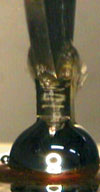
A wetting balance can be used in two modes for testing printed board test coupons; a solder bath, or the preferred method, the solder globule. In the case of the test coupons shown in Figure 2, either individual test pads or oblong pads shown on the bottom of the sample are tested with the globule. Alternatively, the seven pads should be tested simultaneously with a solder bath.

To provide repeatable results the wetting balance may be used to assess changes in solderability on test pads, audit panels or even pre-production boards. Test pads can typically be 2 x 3,5 mm, smaller pads can be used with smaller solder globules to better reflect what is used in the industry, but alignment of the sample is then more demanding on the operator. The author has spent many hours doing testing of this type and it can be demanding.
With modern assembly processes the boards are often subjected to pre-baking, adhesive curing and wave soldering; each will affect solderability to some degree. The board may also have been subjected to a reflow soldering process for topside mounted components. In the case of double-sided products, one or two high temperature reflow processes may also be experienced. The hold time between side one and side two reflow or wave soldering can be assessed. Other process stages known to affect solder finishes include board washing, adhesive curing and handling. In each case the test pads can be used to assess the impact of the previous process stages. It is a useful technique to assess the benefits of nitrogen reflow against running in air; the impact of different levels of nitrogen on solderability performance can also be gauged to reduce costs.
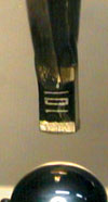
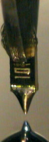
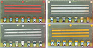
During the author's Lead-Free Experience 3 Workshop, samples were removed from the circuit board featuring a series of seven pads, the edge of each of the pads extended to the edge of the board. This is important to avoid the buoyancy effect that would result if the laminate contacted the solder before wetting the pad. The pre-routed test coupons also featured mouse bit breakout tabs to make removal easier. The board sample is then placed in a modified holder to allow the board sample to be lowered at an angle of 45°. During Experience 3, the testing was conducted on a solder bath rather than a solder globule, using the Menisco solderability system provided by SEHO.
The following parameters were used: 60/40 solder; pure non-activated flux.
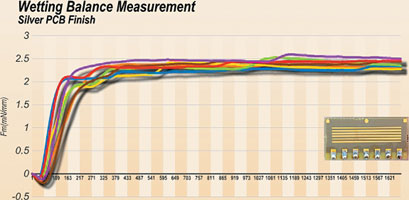
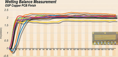
When a solder pellet is used for tests it is conducted at 235°C for tin/lead using a 200-250 mg solder globule on a 2 mm globule block with an immersion depth of 0,1 mm. The immersion speed for the tests are typically 1 mm/s with a dwell time of five seconds. In the case of lead-free, a higher temperature is used. A further benefit of the globule approach is the alloy used for test can be the same as that used in the assembly process. The difference in wetting found between tin/lead and lead-free materials has been highlighted many times.
The 200-250 mg globule may be used on each pad to be tested without contacting the adjacent pad. Due to the size of the pad under test, a new pellet is applied to the block after each test. This is due to the amount of solder removed on each test site. It is also necessary to remove the occasional solder spike from the pads to avoid them touching the globule block, affecting the next test result. Spikes can be caused by poor solderability but often by the cooling effect of the board and its mass. The tests can be conducted using both pure rosin and activated rosin flux to assist repeatability of assessment.
Wetting balance solderability testing experience 4
Although the solder spot test pattern has been used for four years in the Lead-Free Experience, the wetting balance is the standard industry test method and has been developed over the years for PCB assessment using a test coupon with seven test sites shown in Figure 4.
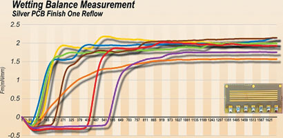
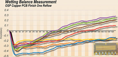
Sample boards from the Experience previously subjected to one or two reflow cycles were tested 10 days after the first reflow by Gen3 Systems. The graphs show the changes in solderability after one reflow operation; the results are exaggerated due to the hold time prior to testing. It is well known that some alternative surface finishes do not hold up to one reflow cycle and extended hold time before the second soldering operation. This is a critical issue when selecting surface finishes. Some companies build their products or contract out the assembly, and only complete the final assembly when orders are received. This situation is often not considered during the evaluation phase.
Test conditions used on the wetting balance:
* Solderability testing conducted with 200 mg SAC pellet.
* One pellet per test site.
* Temperature set point 260°C.
* No hold for pre-heat.
* Speed 0,1 mm/s.
* Flux ACTIEC5.
Using these techniques, assembly companies and printed board manufacturers can use the wetting balance to guarantee the solderability of boards and components in their drive for zero-defect manufacture. The test has often been used by the author for material evaluations, the impact on assembly process stages, the change in flux activity and supplier audits. It is also a useful technique as part of product development or to provide customers with technical support. Use of this test method eliminates the arguments which often arise when the soldering quality does not provide the expected soldering yields in production.
About the author: Bob Willis is a process engineer providing engineering support in conventional and surface mount assembly processes. He runs production lines for suppliers at exhibitions and also provides seminars and workshops worldwide. For further information on how Bob Willis may be able to support your staff, contact him via his website at www.askbobwillis.com


© Technews Publishing (Pty) Ltd | All Rights Reserved
 printer friendly version