


Ref: z2920151m
EDA software tools include simulation, post processing, and physical design. With the exception of the physical design software, the post-processor is the tool designers use the most. The post-processing capability of an EDA software package is crucial for enabling designers to analyse their simulation results, make design decisions, and create documentation. This article covers the characteristics of a post-processor that are present in a world-class EDA software package, and includes many examples.
The process of designing a circuit includes choosing a topology, running preliminary simulations (which may include tuning, parameter sweeps, optimisation, and design of experiments or sensitivity analysis), and running statistical simulations to determine manufacturability. When the device is manufactured, the designer may want to compare how well the actual measured results agree with simulations. The capabilities of the postprocessor determine how efficiently all of these steps may be carried out. If your postprocessor lacks some of these capabilities or they are difficult to utilise, your designs may be under-characterised and sub-optimal. Your design efficiency may be considerably less than that of designers who have access to the full features and capabilities of a leading post-processor (see below: Features and capabilities of a world-class post-processor).
The post-processor is not just about plots, listing columns, and text. It is also the ability of a simulator to take the raw data (voltages and currents) it generates and compute specifications such as gain, conversion loss, ACPR (adjacent channel power ratio), noise figure, etc. A good post-processor will enable you to set up, before the simulation, what you are going to compute, and allow you to create new plots and carry out new calculations on the data after the simulation is finished.
Features and capabilities of a world-class post-processor
A top-class post-processor (or data display) should allow you to:
* Mix equations, plots, and text together. It should have a high degree of flexibility.
* Re-use post-processing setups. Once you have setup your data display to show all the performance characteristics of a mixer, for example, you (or a colleague) should be able to re-use it when designing or simulating a different mixer.
* Place limit lines on a plot to determine whether a design satisfies its specifications or not.
* Plot responses versus swept design parameters to enable you to determine optimal parameter values.
* Plot responses versus multiple variables (such as scatter plots in a statistical simulation) to enable you to determine which design parameters matter the most (and thus require tight control, if possible) and which can be ignored.
* Use markers placed on a trace to compute something else.
* Plot contours of responses versus two different swept variables.
* Perform on-screen editing of the data being plotted, as well as the limits of the x and y-axes.
* Use a marker to select a single value of a swept parameter and plot the response for that single value.
* Keep track of simulation setup conditions and variables and record them automatically for documentation purposes.
* Add text in arbitrary locations, as well as vary the font and size of the text to make it as readable as possible.
* Add a plot legend to enable you to distinguish among multiple traces on a plot.
* Carry out various computations via numerous built-in functions.
* Get started quickly rather than having to re-invent everything from scratch. It should be well documented and have hundreds of examples included with the software or that may be downloaded.
* Easily change plot scales, and zoom in or out on or scroll through data.
* Parameterise traces by variables. For example, change the bandwidth of a computed spectrum by just using on-screen editing to change a ‘bandwidth’ variable.
* Automatically create complex displays that are identical to measurement instrumentation (such as an eye-diagram or vector signal analyser display.)
* Easily export results to spreadsheets or text files.
* Easily compare results from different simulations.
* Place markers on traces that automatically track the maximum, minimum, peaks, or valleys.
* Store traces in history mode, so you can see easily how much a response changes when you modify the design and re-run the simulation.
* Go back and review simulation results at a later date without having to re-run the simulation.
Examples
Here we will illustrate the advantages of a flexible and powerful post-processor data display tool through various examples.
Figure 1 shows the results of an harmonic balance simulation of a VCO (voltage-controlled oscillator), in which the tuning voltage was swept. The steady-state frequency and spectrum for each value of the tuning voltage was computed. The figure shows the steady-state waveforms, spectra, fundamental frequency, and tuning sensitivity. Also included is a plot of the differential output voltage from a separate transient simulation.
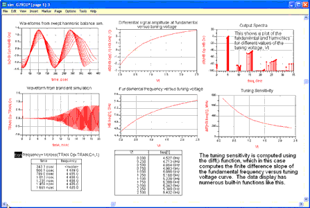
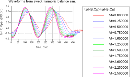
Figure 1 also shows the range of oscillation frequencies, given the tuning voltage range of 0 to 2,5 V, the variation in signal amplitude, as well as the harmonic levels. This display can easily be modified to add or delete plots, re-arrange the layout of the plots, add pages, etc. Figure 2 shows the addition of a plot legend to the plot of the steady-state waveforms.
Figures 3a and 3b show a comparison of the VCO’s tuning characteristics (fundamental frequency versus tuning voltage) when simulated using a lumped-element equivalent circuit for the spiral inductor and when using S-parameters generated by an EM (electromagnetic) simulation of the spiral.
![Figure 3a: Plot results from two different simulation setups, for comparison. Delta marker mode may be turned on to compute the difference more precisely, or you could use an equation: FreqDelta=VCO_wEM_IndModel..freq[1]-HB.freq[1], as shown in Figure 3b](articles/Dataweek - Published by Technews/z2920151mc.png)
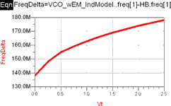
The plot indicates there is a 150 to 200 MHz increase in the fundamental frequency of the VCO when the EM results are used to model the spiral. The red (lower) trace comes from a 'VCO_wLumpedIndModel' dataset (given in the default dataset name field in the upper left corner), which uses a lumped element equivalent circuit, whereas the blue trace comes from a 'VCO_wEM_IndModel' dataset. You may change the data displayed in all the plots at one time by just changing the default dataset name.
Figure 4 shows the variation in fundamental frequency and amplitude versus temperature and tuning voltage. The permute() function is used to change the order of the independent variables, which changes the x-axis variable and enables you to view the same data in a different way. The plots indicate how much more the fundamental frequency varies with temperature when the tuning voltage is near 0 volts than when it is near 2,5 V.
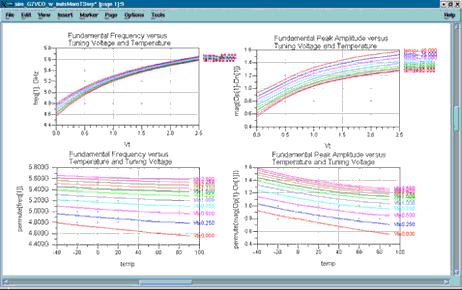
Figure 5 shows the gain, noise figure, input return loss, and reverse isolation of an LNA (low-noise amplifier) simulated under typical conditions and four corner cases. Limit lines for the specifications are included.
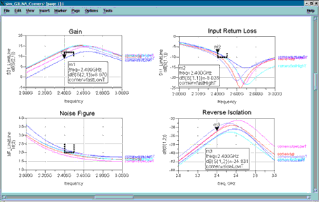
Figure 6 shows noise, available gain, and stability circles, as well as optimal source and load impedances of an LNA device. This plot is parameterised in two ways. There is a marker for selecting the analysis frequency (RF frequency) and a marker GammaS for selecting a source reflection coefficient anywhere on the Smith Chart.
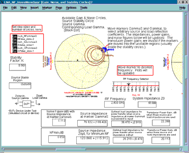
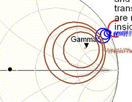
Figure 7 shows a clearer picture of the GammaS marker.
The source impedance corresponding to the GammaS location, as well as the noise figure, the corresponding optimal load impedance, and transducer power gain are all computed and displayed. The equations that carry out these computations are all on a separate page of the data display, which may be modified. You may 'hide' equations you do not need to look at regularly on page 2, for example, and display only the plots and results you need to study on page 1 (there is no limit to the number of pages.)
Figure 8 shows mixer noise figure and conversion gain contours. The contours are a function of the real and imaginary parts of the source impedance.
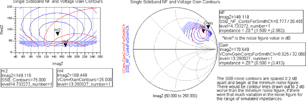
The contours indicate the optimal values for the source impedance, depending on whether you want the minimum noise figure or maximum conversion gain. The contours also indicate how rapidly the noise figure and conversion gain vary with the source impedance. You can easily change the spacing between the contour lines, as well as the number of lines drawn.
Figure 9 shows the frequency response of a baseband, tunable, analog filter, for different values of the tuning voltage, Vt.
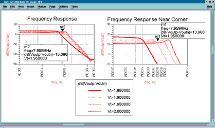
Figure 10 shows the variation in the IP3 (TOI) point and voltage conversion gain versus a swept parameter, GateWidthCS, the gate width of a current source FET.
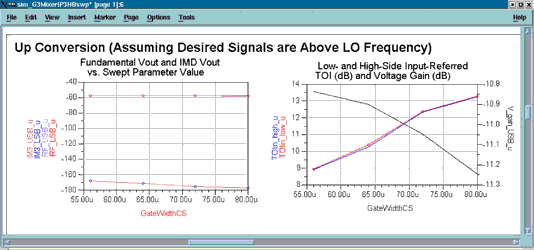
The plot indicates that the IP3 point increases about 4 dB, whereas the voltage conversion gain degrades by about 0,4 dB as the GateWidthCS parameter is increased from 56 μm to 80 μm.
Figure 11 shows the voltage gain and gain compression, intermodulation distortion, and IP3 point calculation versus input signal amplitude.
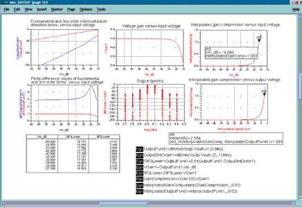
IP3 is computed from a simple geometric extrapolation that assumes the intermodulation distortion terms increase at a 3 dB/dB slope and that the fundamental terms increase at a 1 dB/dB slope. The diff() function is used to make sure this assumption is correct (it is at low enough input signal levels, but clearly not near compression.) Also, the interp() function, which interpolates between simulated data points, is used to obtain higher resolution in the gain compression plots.
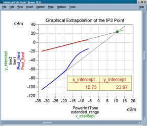
Figure 12 shows a graphical method of extrapolating the IP3 point. Equations placed on the same page are used to calculate the two lines and their intersection.
Figures 13 through 16 are created from several pages of listing columns and plots that are generated automatically by one simulation (called a Wireless Test Bench) using an 802.11b Wireless LAN signal.
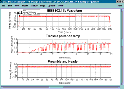
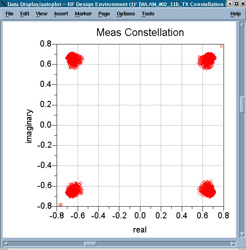
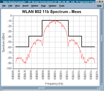
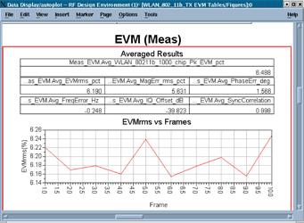
Figure 17 shows load pull simulation contours of constant power delivered and constant power-added efficiency (PAE.) The red Xs show the actually-simulated load impedances. Marker m3 may be moved to any of these Xs, and the PAE, power delivered, and impedance values in the boxes will be updated.
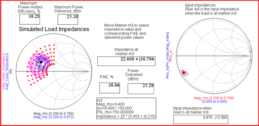
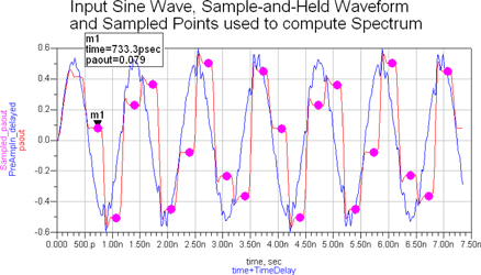
Figure 18 shows several waveforms in a track and hold circuit. The initial sample point from the 'held' waveform is determined by the marker m1 location.
A spectrum is computed from the sample points, shown in Figure 19.
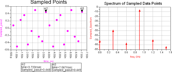
Figure 20 shows another example of the mixture of text, equations, listing columns, and plots to explain the steps required to generate a baseband modulated signal with an arbitrary carrier frequency.
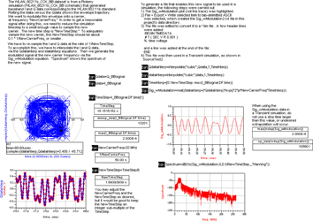
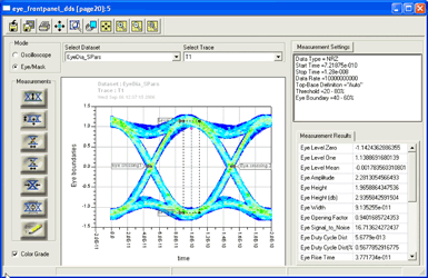
Figure 21 displays and shows measurements on an eye diagram. This display mimics that of an Agilent Digital Communications Analyser. The measurements are derived from the instrument.
Summary
This article has outlined and shown examples of some of the important features and capabilities that should be present in the post-processor of a top-class EDA design software package. All of the presentations are from Agilent’s EEsof EDA, Advanced Design System (ADS), or RF Design Environment (RFDE). The examples shown represent only a small fraction of what the post-processor is capable of doing. For more information about Agilent’s EEsof EDA products, see http://eesof.tm.agilent.com
About the author: Andy Howard, applications engineer, joined HP in 1985 as a development engineer designing microwave circuits. He spent a year in Japan as a systems engineer before becoming an HP EEsof applications engineer in 1993. His applications work has included simulating noise in nonlinear circuits, high-yield design techniques (design of experiments), circuit envelope applications, and Agilent ADS and RFDE examples. He developed the ADS Amplifier DesignGuide, and also worked on the Mixer DesignGuide. He designed a highspeed prescaler IC using Agilent’s RFIC Dynamic Link that was fabricated using IBM’s SiGe process. He is the author of the RFIC Flow Workshop. He graduated from U.C. Berkeley, BSEE, 1983, and MSEE, 1985. He was a visiting researcher for one year at NEC's Central Research Labs in Japan while a graduate student, and is fluent in Japanese. He has published more than 20 magazine articles, HP or Agilent seminar papers, and application notes.
For more information contact Jacqui Saul, RF Design, +27 (0)21 555 8400, [email protected]
| Tel: | +27 21 555 8400 |
| Email: | [email protected] |
| www: | www.rfdesign.co.za |
| Articles: | More information and articles about RF Design |


© Technews Publishing (Pty) Ltd | All Rights Reserved
 printer friendly version