


MMIC and RFIC designers are using spreadsheets that ignore image noise and impedance mismatch. These omissions postpone product launches and hit sales, argues Applied Wave Research’s Chris Paris, but can be overcome with dedicated software that can quickly expose circuits’ weaknesses.
Wireless communications technology serving commercial and defence markets is evolving at a rapid pace. The changes are putting pressure on MMIC and RFIC designers to deliver products with higher data rates and discover the 'killer applications' for cellular, satellite communications, wireless LAN, software radio, and WiMAX markets. For success, products must hit the market ahead of the competition, as the typical lifetime for consumer electronics is only two to three years and a six-month delay can mean a wasted opportunity. Consequently, engineers need to gain a detailed understanding of the RF system fast.

Clinging to the abacus
Unfortunately the electronic design automation (EDA) tools at the system level are inferior to those at the digital and circuit level and have fallen behind the needs of the designer. Engineers are instead relying on spreadsheets, the computational equivalent of the abacus, for a first-hand analysis of system-level performance.
This modern abacus is an effective computational tool but it fails to deliver an in-depth analysis of the RF link performance. This lack of precision means that several cycles of design iterations and breadboard tests are required to hit the desired specifications, which slows the product release and impacts on a company's sales. However, this weakness is not to be interpreted as a criticism of designers who use spreadsheets as their first pass design tool of choice, but a reflection of the paucity of alternative software available over the past 20 years of the wireless revolution.
Another weakness of spreadsheet-based analysis tools is that they eat into the time engineers spend developing communications technology because months are lost to perfecting spreadsheet macros. These are often optimised for a specific structure, which means that time is also required to develop more spreadsheets for analysing new structures. The personalised nature of these spreadsheets is also problematic. If they are passed on to another engineer the recipient can be unaware of idiosyncrasies and caveats contained within the tool, and this can lead to erroneous specifications.
On top of all these flaws, most spreadsheets suffer from one fundamental failing: incorrect calculations of the noise that determines the RF link quality in components such as receivers. This error arises because the calculations for the cascaded noise figure (NF) - the noise that results from a string of RF components connected to form a circuit - use a formula that ignores image noise (see below: What is image noise?) In addition, spreadsheets often omit factors such as phase noise and impedance mismatch between components.
These oversights produce ballpark results of typical cascaded values and a superficial view of RF link performance. Although this can be addressed by manipulating the spreadsheet to account for the missing features, this requires expert knowledge and precious time.
Analysis tool
We believe that a more effective approach to analysing wireless circuit performance involves using Applied Wave Research's RF Budget Analysis tool, released in September 2006. This software, which can run on a standard PC and is part of Applied Wave Research's updated Visual System Simulator (VSS) RF Analysis (RFA) tool, enables designers to make traditional RF cascaded measurements along a communication link of properties such as gain, noise figure and third-order intercept, inclusive of image noise. With this tool MMIC and RFIC designers can also explore the interactions of components within the radio design at the system level before individual components are connected together at the circuit level.
Some of the benefits of our software, which can reduce design cycle times and accelerate product launches, are illustrated in a comparison between two typical MMIC front end receiver links (see Figure 1 for a screenshot that compares the two scenarios). These circuits, which can be evaluated in a matter of seconds, feature two different image noise rejection filters in links that also contain a bandpass filter, low-noise amplifier (LNA), quadrature mixer, low pass filter and a 50 Ω terminating load.
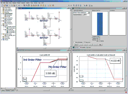
The seventh-order image noise rejection filter produces an RF link with a 3,4 dB NF, 0,2 dB lower than that using a third-order filter. However, it has the penalty of a higher component cost and a similar performance at a lower price might be produced with a third-order filter and an LNA with less noise.
Both of these scenarios can be evaluated within a few minutes with our software that can also provide a yield analysis and keep track of changes in other figures of merit - for example, the available cascaded gain at the image frequency changed from -6,22 dB to -32,9 dB by switching from a seventh-order to a third-order filter. This example demonstrates some of the benefits of commercial system simulation tools, which can account for real world circuit interactions and make it easy for a designer to perform trade-off studies.
Another component of the VSS RFA package is the RF Inspector technology tool, a new frequency-domain simulation tool that helps to determine the causes of any inter-modulation product in an RF link. This tool, which is based on a new set of algorithms, takes into account the effects of conversions, harmonics and intermodulation, and includes thermal and phase noise. The tool can identify contributions from every component in the circuit to unwanted signals, which allows designers to tackle the most significant problems first.
The advantages of this tool are demonstrated by examining a circuit that could feature in 3G cellular, WiMAX or WLAN applications, which down-converts a desired signal at 2,1 GHz to an intermediate frequency (see Figure 2a). This circuit is subjected to two unwanted signals at 1,4 GHz and 2,4 GHz that cause interference and can replicate undesired signals generated by other applications. Our RF Inspector evaluates the effects of these unwanted signals and reveals the repercussions of improper filtering before down-conversion. Placing a marker over a particular tone of interest shows the associated power level and signal heritage at that frequency.
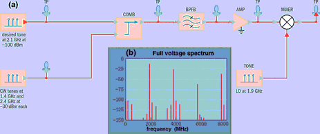
The tool can monitor the full frequency spectrum, the spectrum of only the signal, the phase noise of the RF link or just the effects of the thermal noise (see Figure 2b). The data can also be replicated as a table that uses flags of different colours to identify the desired signal, inter-modulation and distortion products.
We believe that the ability to expose the weaknesses in circuits with the RF Inspector, combined with the circuit performance analysis offered by our RF budget analysis, enables circuit designers to create and verify the initial specifications of a wireless design and identify potential pitfalls at an early stage of the design process. This will ultimately shorten the design cycle and boost company revenue by increasing the pace at which products are brought to market.
What is image noise?
Image noise is a consequence of the nature of simple analog multipliers or mixers that do not preserve polarity. This noise is seen in a typical ‘down-conversion’ process, which produces the signal at the centre frequency from the difference between the mixer’s local oscillator frequency and the input frequency. This centre frequency also features a contribution from a higher frequency, referred to as the image frequency, which produces a signal at the centre frequency when down-converted. Not accounting properly for image frequency can lead to serious consequences. The amount of image noise that is added is dependent on how much of the image frequency band is present at the input of the mixer and its effects can be reduced with image noise rejection filters.
About the author
Chris Paris is director of European operations at Applied Wave Research. He thanks Joel Kirshman, product manager for AWR system analysis tools, for his technical contributions.
| Tel: | +27 11 314 4101 |
| Email: | [email protected] |
| www: | www.dscoms.com |
| Articles: | More information and articles about DS Communications |


© Technews Publishing (Pty) Ltd | All Rights Reserved
 printer friendly version