


Motivated by the belief that people should have a choice, Baskin-Robbins, a global chain of ice cream parlours, opened in 1945 with 21 flavours, an innovative concept at the time. In 1953, the store kicked off its famous ‘31 Flavours’ slogan, representing a flavour for every day of the month. More than 60 years later, the chain now offers more than 1000 unique flavours of ice cream.
For today's designers using programmable logic, the unrelenting claims of low-power leadership can be as confusing as walking into Baskin-Robbins, only to find out that all the tags have been removed from the containers. You peer through the glass, trying to discern what is in each one. You spot vanilla, but is it regular, French or sugar-free?
What is the difference between the offerings? How can you determine the best 'low-power' field-programmable gate array (FPGA) for your power- and cost-sensitive application? As with most engineering decisions, the final answer depends greatly on your specific design constraints, among which are likely to be power, performance (or speed), logic and I/O count. The final choice of the most suitable FPGA device for your application is usually best framed in the context of these requirements.
A proliferation of power- and cost-sensitive designs
The tremendous growth in battery-operated and power-sensitive applications has created a global demand for low-power semiconductors. Today's power-sensitive designers face stricter system power limits, specifications and standards that put a cap on the total power consumed by the system. Simultaneously, for these applications, the demand for increased features, performance and complexity continues to grow, but not at the expense of draining the battery or increasing costs.
Designers have traditionally relied on application-specific integrated circuits (ASICs), not FPGAs, to meet their low-power constraints. With longer time-to-market, rising non-recurring engineering charges (NREs), and a lack of flexibility to address changing standards and late-stage design modifications, hardwired ASICs are riskier and often impractical for applications with short product life cycles. As a result, PLDs are becoming the preferred solution as competition intensifies and time-to-market has an increasingly greater impact on product success.
In fact, more and more, designers are finding that a low-power, reprogrammable solution is required to adapt to evolving standards, speed time-to-market, and deliver the footprint and power consumption required for the next cutting-edge silicon solutions. Market research firm iSuppli predicts that as much as $3 billion of the estimated $20 billion ASIC market could potentially shift to low power FPGA solutions.
The many flavours of 'low-power' FPGAs
Certainly not all programmable logic is well suited to address low-power needs. In fact, some of today's 'low-power' FPGAs draw upwards of 30 mA, which is often an order of magnitude or two higher than typical power-sensitive, battery-operated applications can tolerate. At startup, SRAM-based devices experience well-documented inrush and boot-up configuration power spikes during system initialisation that can cause excess battery drain.
Alternatively, single-chip, Flash-based devices do not require an external configuration device (ie, boot PROM or microcontroller) to support device programming at every power-up cycle, and the live-at-power-up feature eliminates the need for an external device to assist in system power-up. Removing the additional parts required by SRAM-based FPGAs not only reduces board space and system power consumption, but also increases reliability, simplifies inventory management and lowers total system costs by as much as 70% compared with similar SRAM-based FPGA solutions.
Once the FPGA is on and configured, power consumption takes two basic forms - static and dynamic (also called active). Static power consumption is the current drawn by the FPGA when it is powered up, configured, and doing nothing; dynamic power is consumed when devices are actively working.
Until recently, dynamic power was the dominant source of power consumption. Once helping to manage the dynamic power problem, device supply voltages (VCC) had scaled downward with process shrinks and subsequent lower system voltages, but the days of continued scaling are gone.
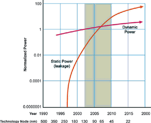
Compounding the issue further, is that each process node shrink means additional static power consumption for transistor-heavy SRAM based FPGAs. This is due to worsening problems such as quantum tunnelling and sub-threshold leakage, which create real challenges for devices targeted at power-conscious applications. And, with leakage worsening, static power has begun to dominate the power consumption equation as the biggest concern. Figure 1 illustrates the increasing contribution of static power at shrinking process nodes.
To address some of these power concerns, several suppliers of SRAM-based FPGAs claim to offer 'single-chip,Flash-based' solutions. These 'hybrid' solutions are merely combinations of Flash memory components with the underlying SRAM FPGA technology - either integrated with the FPGA die into a single package or, alternatively, stacked or placed side-by-side. Unfortunately, the FPGA array is still volatile and is subject to the power drawbacks associated with these types of devices. With these solutions, the embedded Flash memory blocks control only the initial configuration of the devices during power-up.
True non-volatile FPGAs are those that contain a non-volatile FPGA array, enabling significantly reduced power consumption, improving response times and delivering unparalleled reliability and uncompromising security.
Both the silicon-in-package (SIP) and the multichip package (MCP) hybrid approaches overcome some of the limitations of traditional SRAM-based solutions by providing a smaller footprint, a minor reduction in power consumption and small advances in power-up time and security. But these are only incremental improvements over their pure SRAM-based peers. In some cases, these devices have been proven to consume 1000 times more static power than true Flash-based FPGAs.
Because true non-volatile flash-based FPGAs do not use millions of power-hungry SRAM configuration bit cells, they have significantly lower static power than SRAM-based solutions, making them ideal for power sensitive applications. In fact, the many flavours of Flash-based, low-cost FPGAs include devices that have been optimised for power, speed and I/O, some of the fundamental design requirements for power- and cost-sensitive design.
An FPGA flavour for every occasion
Actel offers several families of FPGAs, each catering to specific sets of design requirements.
The IGLOO family is optimised for low static power consumption, thought to be the industry's lowest power programmable solutions at 5 μW. The family supports up to 250 MHz operation and offers 1,2 and 1,5 V operation, densities up to 3 million system gates, and enhanced features such as PLLs, RAM and user non-volatile memory. Additional advantages of the devices include flexible power-saving modes with rapid recovery to operation, low dynamic power consumption and clock management. Available in a 4 mm package with a 0,4 mm ball pitch, IGLOO FPGAs are particularly attractive for applications where low power and small size are critical.
Flash-based, 5 μW IGLOO Plus FPGAs have been optimised for I/O-intensive applications, particularly those employing I/O-intensive memory bus manipulation, general-purpose I/O expansion, sequencing, interface translation, storage, and touch screen and keypad technology.
For designers of high-performance, power-conscious systems, the ProASIC3L family of FPGAs combines 40% lower dynamic power and 90% lower static power than its previous-generation ProASIC3 FPGAs, with up to 350 MHz operation. As a result, designers in high-performance market segments such as industrial, medical and scientific, now have access to flexible, feature-rich solutions that offer speed, low power and low cost.
The 1,5 V ProASIC3 FPGAs are optimised for performance. Featuring 350 MHz operation, the one-million-gate ProASIC3 A3P1000 FPGA, for example, delivers standby current consumption of only 8 mA under typical conditions. Low-power applications that require 32-bit processing can use the ARM Cortex-M1 processor without licence fee or royalties in M1-enabled ProASIC3 devices, providing the benefits of programmability and time-to-market at an ASIC-level unit cost.
For more information contact ASIC Design Services, +27 (0)11 315 8316, [email protected], www.asic.co.za
| Tel: | +27 11 315 8316 |
| Email: | [email protected] |
| www: | www.asic.co.za |
| Articles: | More information and articles about ASIC Design Services |


© Technews Publishing (Pty) Ltd | All Rights Reserved
 printer friendly version