


The never ending quest to jam ever more functionality into smaller and smaller packages has increased the popularity of yet another high performance device that is quickly gaining favour among handheld product designers and manufacturers. It is the QFN: an abbreviation that stands for quad flat no-lead.
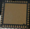
First patented in 1999, use of the QFN has steadily increased in recent years, especially with the proliferation of smaller multifunction handheld devices. QFNs (pictured) are just as the name describes: a flat plastic package with perimeter leads underneath the device and a large pad in the centre. Basically, it is a QFP (quad flat pack) with no leads, and the connections are made by soldering the perimeter lands underneath directly to the pads on the printed circuit board (PCB). In addition to their small form factor advantages, QFNs offer excellent electrical and thermal performance.
While these devices provide clear benefits there are, of course, some challenges as well.
At the package level, there are manufacturing hurdles to overcome, such as issues with wire bonding on polyimide and the die to pad ratio effect on JEDEC performance and, once the devices are made, the next challenge is assembling them onto the PCB and ensuring the long term reliability of the assembly.
For the purposes of this discussion, we will focus on the assembly issues and how to best resolve them. Though the geometry of the QFN is, in part, what makes it appealing, it is also the cause of one of its greatest assembly problems: voiding. When you couple a QFN with a lead-free process, the issue of voiding becomes even more problematic. Here is why.
There are arguably many variables that contribute to the increased voiding characteristics of SAC alloy solder joints. Strictly speaking from a materials perspective, though, the problem has to do with the proclivity of SAC materials for volatile formation. SAC alloys form more gases and these volatiles cannot escape as easily from a molten SAC alloy as they can from a conventional SnPb alloy. They have to travel a greater distance to escape and, therefore, become trapped inside the solder joint and form voids.
When this condition is combined with the unique geometry of the QFN, voiding may become even more prevalent. Unlike BGAs where there are bumps or a QFP where there are leads, the QFN provides no standoff so there is nothing to absorb stress or allow for volatile escape. What is more, the pad in the centre of the QFN, which is primarily used for thermal transfer, presents large area soldering challenges and, consequently, issues with voiding. Because there is such a large surface area and no standoff to allow volatiles to escape, these gases may become entrapped and cause void formation.
Though many would argue that some level of voiding is acceptable, Henkel's stance has always been that reducing voids as much as possible is the best approach. Plus, with QFNs, the voids are not just problematic from a mechanical perspective, but can also result in thermal transfer impedance issues as well. This can lead to resistive heating and, if the voids are sizeable, hot spots can develop and may lead to thermal damage of the device.
Resolving the QFN voiding challenge may not be as difficult as it seems, however. Through a two-pronged materials-based and process-based approach, the materials experts at Henkel have successfully reduced the incidence of voiding in QFNs in both laboratory and high-volume production environments. Henkel's work has revealed that modifications to the solder paste flux system can significantly reduce void formation.
The flux's solvent concentration and boiling temperature, flux content and flux activator concentration all play a role in volatile formation. By altering the flux system to reduce volatile generation, voiding is lessened significantly. Using this technique, Henkel has developed some innovative, low-voiding solder pastes aimed at enabling the QFN to be the powerhouse package it was intended to be.
A low-voiding solder paste in combination with optimised reflow profiles is clearly the best method for ensuring void reduction. I would be remiss if I did not also mention the potential impact of varying the print patterns for the QFN's centre pad as another possible void reduction mechanism.
Depending on the size of the device, limited success has been realised through printing a pattern - such as a snowflake or cross - instead of covering the entire pad with paste, which may allow for some area through which gases can escape.
While we have successfully shown that using a low voiding solder paste and an optimised reflow profile are the best proven routes to QFN void reduction, more detailed analysis of QFN voiding behaviour is certainly warranted to fully understand this issue. In fact, Henkel and Technology de Monterrey recently launched a year-long study on QFN assembly and we expect to publish the final results by year's end.
| Tel: | +27 11 869 0049 |
| Email: | [email protected] |
| www: | www.mykaytronics.co.za |
| Articles: | More information and articles about MyKay Tronics |


© Technews Publishing (Pty) Ltd | All Rights Reserved
 printer friendly version