


Power consumption today is among the most crucial considerations in electronics design. From concerns about building systems that use too much energy to crafting portable devices that last days on a single battery charge, engineers are intently focused on optimising their power budgets.
Consider that, at the macro level, in North America growth in demand for electricity has outstripped generation supply by 25% per year since 1982. Homes have more power-hungry devices (computers, routers, displays, printers and so forth) than ever.
At the micro level, the smaller and more powerful devices being designed to enable these systems are running into power management problems the more sophisticated they become. Some experts, for example, have estimated that each process generation increases semiconductor device leakage current by a factor of 10. Often, leakage can be more than half of total power consumption.
Power has risen to the No. 1 or No. 2 concern in contemporary engineering surveys as more devices – from medical equipment to cellphones to portable music players – go mobile. The solution, until recently, was simple: select an application-specific integrated circuit (ASIC) that engineers could optimise for power. The size of the potential market justified the upfront engineering cost because it would be amortised over hundreds of millions of units.
But the frequency of that choice has declined in recent years. Consumers are demanding more features and functionality in their devices more quickly, and that shrinking product life cycle (with attendant smaller unit volumes) has squeezed ASICs as a solution.
As the spotlight has turned to the more flexible and fast time-to-market FPGA devices, the concern about the programmable device’s power history has become evident. But innovation has quickened in the programmable logic space. Gains in architecture and process technology have wrung out advances in performance and cost, yielded smaller, better packages, and reduced power consumption.
New device families now open a world of design choices for system engineers who no longer have to compromise on their power budgets when using an FPGA.
The art of low-power design
Depending upon the type of FPGA technology chosen, power consumption can be composed of as many as five different factors: static power, dynamic power, power-on inrush current, configuration power and sleep (low-power) mode power.
Static and dynamic power are familiar concerns for all integrated circuit (IC) designers. Static power is dominated by leakage current in several forms: sub-threshold leakage, junction leakage, gate-induced drain leakage and gate leakage. Dynamic power refers to power consumed during device operation and correlates with such factors as used functional resources (logic blocks, clock trees, embedded RAM, PLLs, etc), loads and resistive terminations on I/Os, data patterns and their arrival dynamics, signal activity or toggle rates, and signal static probabilities.
Designers considering volatile, SRAM-based FPGA solutions must also consider three other components of power. Inrush and configuration power consumed during system and device functional power-up, as well as power required during sleep mode can be significant for these devices, as illustrated in Figure 1.
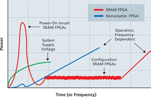
Despite the efforts of SRAM-based FPGA vendors, these power components remain and can significantly increase power consumption, especially when several FPGAs populate a single board or use power from a common supply on different boards. The impact is greater for systems with frequent on/off cycles and must be considered when estimating battery life. Thus, when sizing power supplies or selecting batteries for SRAM-based programmable devices, board designers must account for configuration and in-rush power dissipation.
Another measure taken by FPGA makers to remedy transistor leakage is to create cells with two levels of threshold voltage (VT). This so-called multiVT technique seeks to reduce overall design leakage by deploying a minimum of more leaky low VT devices, while maximising the use of less leaky high VT cells. MultiVT has been employed in the past in ASIC and application specific standard product (ASSP) offerings, and is now being adopted by FPGA vendors.
Other power-saving design techniques
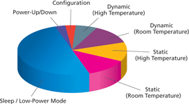
Power optimisation can be managed in a variety of ways (Figure 2). Selective power-down simply refers to shutting the power down to certain portions of a chip, or to certain chips on a board. This can be accomplished by implementing a multisupply strategy in which the power grid of some blocks is de-correlated from others in order to allow for selective shutdown. Power-down or sleep modes within the FPGA architecture can also be deployed to selectively power down blocks when not in use.
Macro optimisation can also yield power savings. Some logic elements are offered in multiple versions optimised for high performance, high density or low power. High-performance macros tend to consume more power than other versions, so power can be saved by deploying high-performance macros only when they are required. For example, a fast adder consumes more power than a slower ripple adder. Examination of the differences between them might reveal that the ripple carry adder consumes about one-tenth of the dynamic power compared to the fast adder.
Dynamic voltage scaling is another power-saving design technique. Since power scales proportionally with the square of voltage, reducing supply voltage can significantly impact power efficiency. If system requirements demand more performance than low-voltage I/Os can deliver, utilising low-voltage I/Os on non-performance-critical pins and higher voltage I/Os for critical signals offers an excellent alternative.
Empowering systems designers
Nowhere is the intersection of power, portability and device size more important than in medical electronics. According to analyst firm, Gartner Dataquest, in a report published in September 2008, the medical electronics market for semiconductors was estimated to be approximately $3,42 billion in 2008. By 2012, this number is expected to reach $4,48 billion, with FPGAs making up more than $323 million of that total.
Medical manufacturers are moving entire systems into palm-sized, portable units requiring high levels of integration, low power, small footprint and high reliability to meet battery specifications and reduce design footprint. For Actel’s part, power optimisation research has yielded the nano families of FPGAs, which have pushed power consumption down to as low as 2 μW. And that is with no sacrifice of density (some families range up to 3 million gates), cost or size (3 x 3 mm packaging).
In an insulin pump, for example, this type of design approach can help absorb additional glue logic and multiple functions – from human machine interface (HMI), display, storage and communication control to microcontroller functions – into a single chip, thereby reducing bill-of-materials, board area, power consumption and cost.
Conclusion
Designing for low power starts with informed FPGA technology and device selection. Leading FPGA companies are introducing power-friendly FPGA architectures and EDA vendors are stepping up with more sophisticated architectural and power analysis tools.
Good design practices, such as well-considered use of clock trees to minimise capacitance, controlling clock networks with gated clocks, exploiting power saving capabilities, and floor-planning the design to reduce the overall span of the clock domain lay the framework for a power conscious design. Power aware design tools can aid these design practices by automating power analysis, remedying problem areas and optimising layout. Armed with these strategies, techniques and tools, the FPGA designer can reduce power and ultimately play an important role downstream in larger energy issues, such as battery conservation and energy independence.
| Tel: | +27 11 315 8316 |
| Email: | [email protected] |
| www: | www.asic.co.za |
| Articles: | More information and articles about ASIC Design Services |


© Technews Publishing (Pty) Ltd | All Rights Reserved
 printer friendly version