


The embedded market continues to move toward 32-bit processing. At the same time, the market has seen a significant increase in the use of FPGAs as flexible, cost-effective platforms for the rapid design of high-performance embedded systems.
In combination, these trends are driving demand for 32-bit processors in programmable logic. Certainly, there is no end to the number of new 32-bit processor architectures. However, most processor intellectual property (IP) is developed for ASIC implementation. As a result, when implemented in the coarse-grained architecture of FPGAs, the processors are often large and slow – a fate suffered by many widely used processors when ported to programmable logic.
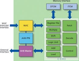
Of course, a few soft proprietary IP processor solutions are available for FPGA implementation. However, only limited tools, support and designer experience exist for these proprietary solutions, making them harder and riskier to use. To address the need for an FPGA-optimised, 32-bit processor based on an industry-standard architecture, Actel and ARM developed the 32-bit Cortex-M1 processor (Figure 1), the first ARM core designed specifically for FPGA implementation.
When combined with Actel non-volatile M1-enabled ProASIC3 FPGAs and Fusion programmable system chips (PSCs), the small, fast and highly configurable Cortex-M1 processor offers a number of benefits. Because the Cortex-M1 processor is available from Actel free of licence fees and royalties, the combination of a low-cost FPGA and the Cortex-M1 processor extends the ARM architecture to lower-volume applications, provides a lower-cost entry into system-on-chip (SoC) design, and shortens time-to-market for ARM users. For designs that scale to ultra-high volumes, the 32-bit Cortex-M1 processor runs the Thumb-2 instruction set and is upward-compatible with the Cortex-M3 processor, providing an easy migration path to ASIC implementation. The Cortex-M1 processor also enables economical re-use of tools, code and knowledge, which reduces risk and gets products to market sooner.
An industry-standard solution designed for FPGA implementation
The challenge associated with proprietary architectures lies in making them efficient in targeted applications and putting tools in place to support them. Experienced engineers know that there is a learning curve when using anything new; it takes time to climb the learning curve and gain the experience to effectively deal with the product’s unique characteristics. This is in direct conflict with ever-shortening development schedules and increases design risk. For these reasons, designers tend to re-use what they are familiar with or what they have used before. Over time, this causes a few architectures to become widely used industry standards, while most are only used in narrow vertical niches.
When investigating which 32-bit processor would best suit customer needs in its flash-based FPGAs, Actel realised early on that an industry-standard architecture offers significant benefits over a proprietary architecture. Industry-standard processors have a broad selection of development tools, a significant volume of available program code, and a large following of design engineers who have knowledge and experience using them. These benefits enable users to get their designs developed faster and to market sooner while reducing risk, and as a result, offer customers a better solution and value.
A unique business model – FREE
When Actel and ARM developed an optimised version of the ARM7 processor for use in Actel FPGAs, it was offered with an innovative business model that dramatically increased industry access to the ARM architecture. By removing the licence, royalty fees and contracts typically associated with licensing models for industry-leading processor cores, Actel offers free access to advanced ARM processor technology for the broad marketplace. The same free delivery model is offered with Cortex-M1 for use in Actel Flash-based, M1-enabled Fusion and ProASIC3 FPGAs. This provides all embedded designers with access to programmable flexibility and system-level integration with the ARM architecture, enabling the development of low-cost, high-performance systems.
Cortex-M1 features
Derived from the ARM 3-stage Cortex-M3 processor pipeline, the highly configurable Cortex-M1 processor provides a good balance between size and speed for embedded applications. The core in its smallest configuration is less than 5% larger than the Actel Core8051, an industry-standard 8-bit controller. It runs at over 70 MHz in Actel M1-enabled ProASIC3 and Fusion devices. The processor runs a subset of the new Thumb-2 instruction set and features support for tightly coupled memory and a sophisticated low-latency interrupt controller to improve embedded performance and capabilities.
Improved code density with performance and power efficiency
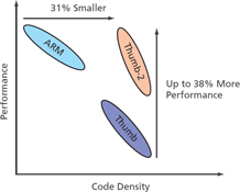
The Thumb-2 new instruction set for the ARM architecture provides enhanced levels of performance, energy efficiency and code density for a wide range of embedded applications. Thumb-2 technology builds on the success of Thumb, the high-code-density instruction set for ARM microprocessors, to increase the power of the ARM microprocessor core available to developers of low-cost, high-performance systems. The technology is backward-compatible with existing ARM and Thumb solutions, while significantly extending the features available to the Thumb instruction set. This allows more applications to benefit from the code density of Thumb. For performance-optimised code, Thumb-2 technology uses 31% less memory to reduce system cost, while providing up to 38% higher performance than existing high-density code, which can be used to prolong battery life or to enrich the product feature set (Figure 2).
Cortex-M1 executes the ARMv6-M instruction set, which is a full subset of the Thumb-2 (ARMv7) instruction set that is used across the rest of the Cortex family. ARM recognises the benefit of having a large volume of legacy code available for customers to use, so they made the Cortex family upward compatible with Thumb code written for their legacy cores (ARM7, ARM9 and ARM11). Existing Thumb code can be run without change on Cortex-family processors, including Cortex-M1 devices. This is a big advantage for designers.
Most of the important processing on legacy ARM processors was done in subroutines written in Thumb code, so designers can take advantage of their existing code for ARM processors. One of the benefits of Thumb-2 over previous ARM instruction set architectures is that 16- and 32-bit instructions are executed in the same mode. In older ARM architectures, Thumb instructions were primarily used in subroutines with the 32-bit ARM instructions used to service interrupts. This often resulted in long latency between the time an interrupt was received and the time it was serviced.
In Thumb-2, ARM merged the 16- and 32-bit operating modes so that interrupts could be serviced without the need to switch from 16-bit mode. It is a big advantage to be able to freely mix 16- and 32-bit instructions. This greatly simplifies the programming task and eliminates the need to profile the code to minimise code size and maximise throughput. It also results in increased performance, because the instructions can be optimally mixed without having to cluster them in 16- and 32-bit groupings.
Fast memory access improves performance
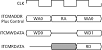
Cortex-M1 has a separate memory interface from the external AMBA (advanced microcontroller bus architecture) peripheral bus interface. This is similar to the high-performance ARM9 architecture but different from ARM7, which has a combined memory and peripheral bus. The separate memory interface on Cortex-M1 is actually implemented as two interfaces, giving separate access to instruction and data tightly coupled memory spaces (ITCM and DTCM). This increases the performance of the processor, because it can fetch an instruction from the ITCM on every clock cycle (Figure 3), and it is never stalled due to data memory accesses, or reads and writes to the peripherals on the AMBA bus.
Efficient interrupts reduce latency
A configurable nested vectored interrupt controller (NVIC) is available on Cortex-M1 that facilitates low latency interrupt and exception handling and simplifies programming. The NVIC supports re-prioritisable interrupts and is closely coupled to the processor core to support low-latency interrupt processing and efficient processing of late-arriving interrupts. In many applications, especially those that operate in realtime, low interrupt latency is critical. The NVIC in Cortex-M1 also gives users the option of individually determining the priority of interrupts, supporting four interrupt levels, allowing designers to give a system event priority over other events. All of the capabilities built into the NVIC give users maximum control over how the processor responds to events as they occur in an application.
Simplified programmer’s model eases coding
Cortex-M1 implements a subset of the Thumb-2 architecture with two operating modes – thread mode and handler mode. For normal processing, thread mode is entered through reset or exception return. The handler mode is entered as the result of an exception. The processor is designed for embedded applications where additional operating modes are not necessary. By limiting the programmer’s model to a few operating modes, the size of the processor has been significantly reduced.
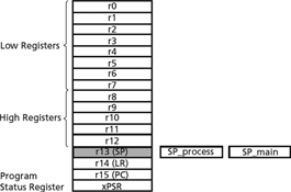
To ease programming and make transition between thread mode and handler mode as seamless as possible, the processor has two stacks (Figure 4). Out of reset, all code uses the main stack. An exception handler can change the stack used by thread mode from the main stack to the process stack by changing the value it uses on exit. The stack pointer, R13, is a banked register that switches between the main stack and the process stack. The processor has been architected to maximise the designer’s control over the flow of data and processing through the core and to simplify programming, especially when different engineers do the software and hardware development.
Implementation in Actel M1-enabled FPGAs
FPGA usage is growing in part because of the flexibility that these devices offer. Engineers can tailor the function of a device exactly to their application by adding or removing soft IP. This is similar to what can be done with an ASIC. With FPGAs, however, a design can be developed and running in the application within a few hours, whereas ASICs require many months and large up-front, non-recurring engineering (NRE) charges.
When developing Cortex-M1, ARM and Actel made the processor highly configurable. The tightly coupled memory size, the size and speed of the multiplier, the number of external interrupts, the endian-ness, and whether the debug circuitry and OS extensions are included are all selectable by the user. This gives designers the control to select the minimum processor configuration that best meets their application requirements.
Furthermore, because Cortex-M1 is being implemented in an FPGA, designers can quickly configure the core and program it into an M1-enabled, Flash-based device and test it in their end application. If a change is required, it can be modified and reprogrammed into the device within minutes. In this way, engineers can modify and test their design many times within a few hours to find the optimal implementation for their product.
The M1-enabled Actel FPGAs allow seamless use of the Cortex-M1 processor core. The M1-enabled ProASIC3 and Fusion devices offer all the benefits of Actel non-volatile, Flash-based families – single-chip, reprogrammable, live-at-power-up, secure, firm-error immune and low-power.
| Tel: | +27 11 315 8316 |
| Email: | [email protected] |
| www: | www.asic.co.za |
| Articles: | More information and articles about ASIC Design Services |


© Technews Publishing (Pty) Ltd | All Rights Reserved
 printer friendly version