


When designing a small wireless sensor node to be powered by the popular CR2032 coin cell, some sources claim there is a 15 mA ‘limit’ and that drawing more current is not possible or will damage the battery. This may give the impression that at 15 mA everything works perfectly and battery capacity is great, while at 16 mA nothing works.
There is little public information available to explain why such a limit exists (if it indeed does exist), and little information explaining why 15 mA would be a ‘magic number’.
Testing peak currents
With the specific protocol of Bluetooth Low Energy (BLE) in mind, an experiment was set up to test the impact of pulsed loads. Although the examples in this article are derived from BLE, it is equally applicable to other low-power RF protocols like ZigBee, RF4CE and similar.
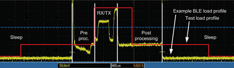
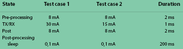
A common BLE load profile can be simplified to have four states: sleep, pre-processing, RX/TX and post-processing. The current drawn during each of these states will vary to some degree, but especially during the RX/TX state. In the testing in question, a load profile was created that resembles a BLE profile. However, to reduce testing time it exceeds the BLE load profile. Figure 1 shows an example BLE profile and the testing profile (red line). The graph scale is 5 mA/div and 400 μs/div.The load profile used in testing is given in Table 1.
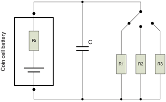
To further simplify the test setup, a switching resistor network was created and each resistor was dimensioned to sink the stated current for a voltage of 2,5 V. A battery’s end of life was determined when the voltage dropped below 2,0 V. Figure 2 is a visual representation of the schematics used for testing and modelling.
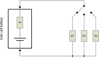
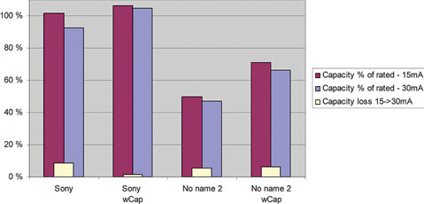
Figure 3 shows the ratio between effective and rated capacity results from a number of vendors. From each vendor, at least 12 batteries were used in testing since the battery-to-battery variation can be quite large. Rated capacity is 220 mAh for all branded vendors; the ‘no name’ vendors did not specify so same rated capacity was assumed.
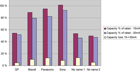
Based on these results, the assumption of 220 mAh capacity for the ‘no name’ vendors might have been too harsh. From these results, two conclusions can initially be made:
A. The difference in effective capacity between 15 mA and 30 mA peak current is not very significant. Average capacity loss is 9%.
B. Effective capacity for both 15 mA and 30 mA peak will be very poor when using batteries from some vendors. Some vendors, including some branded name vendors, only achieve approximately 50% of rated capacity for both 15 mA and 30 mA peak current.
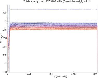
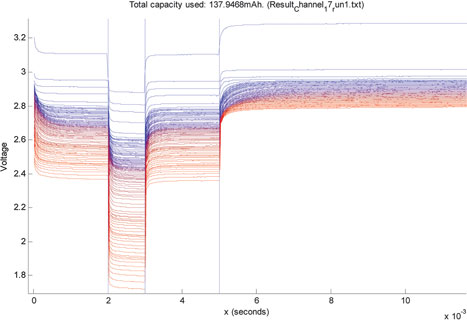
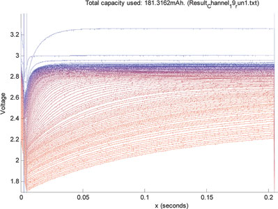
For consistent performance, (B) is more significant than (A). So to ensure consistently good performance, (B) is the main concern and the focus for attention. Clearly, limiting peak current to 15 mA is not sufficient for consistently obtaining good effective battery capacity. Figures 4 and 5 show the voltage during load as the battery is drained, for a 30 mA peak current load for one of the ‘no name 2’ batteries. The colour changes from blue to red as battery capacity is consumed.
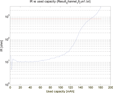
It can be seen that the voltage drop caused by the battery’s internal resistance (IR) during peak load is limiting the effective capacity. Figure 6 shows a typical curve for the calculated internal resistance and how it changes as capacity is used. The red line indicates when the voltage dropped below 2,0 V.
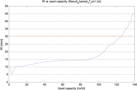
Since the IR increases rapidly as capacity is used, the circuit must be able to manage a very high IR to achieve effective battery capacity. The steep incline in IR also gives a good explanation as to the relatively small difference in effective capacity between 15 mA and 30 mA peak current load. In this testing, the IR limit for 30 mA peak is approximately 30 Ω, and for 15 mA peak is approximately 60 Ω.
How to survive a high internal resistance
A common technique to handle high peak currents is to use a capacitor to offload the power source. During high current periods, the capacitor will act as the primary power source, while during low current periods the battery will be the primary power source and recharge the capacitor. When dimensioning the capacitor it is important to know the battery’s internal resistance and the load profile. With this information it is quite simple to dimension a suitable capacitor.
For this testing, an IR of 1 kΩ was dimensioned for, which resulted in a capacitor of approximately 100 μF. In a low-cost application, this capacitor size would probably be to large or too expensive, but in a real BLE application the capacitor can be significantly reduced by a factor of 2 to 5 depending on application, since the load profile is much gentler. The resulting schematic is shown in the Figure 7. The experiment tested adding a capacitor using the Sony and ‘No Name 2’ batteries since they represent the best and the worst. Figure 8 shows the result.
Although the ‘No name 2’ batteries still do not achieve 100% of rated capacity, it is still a solid >40% improvement. It can also be seen that the difference between 15 mA and 30 mA peak remains at the same level. The Sony batteries increased their effective capacity by 5% and 13% respectively to an almost identical effective capacity. In a real BLE application, the increase in effective capacity is most probably even higher for the low performing batteries since real BLE applications will have considerably longer sleep states and much lower average current consumption.
Figures 9 and 10 show the voltage during load as the battery is drained for the ‘No name 2’ batteries. Figure 11 also shows IR and its increase as battery capacity is used. This shows that with the added capacitor, the circuit is able to manage high IRs.

Dimensioning the capacitor
To simplify the dimensioning of the capacitor, a few simplifications need to be made:
A. During the high current states the battery voltage is fixed at Vmin. This will cause an error on the safe side, meaning that the battery will deliver slightly more energy than calculated.
B. The current consumed by the circuit during the sleep state is normally in the 1 μA range and is therefore omitted.
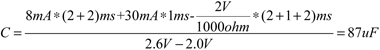
To calculate the capacitor value, focus on the high load states (processing and RX/TX). The formula is given as:
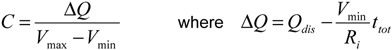
Qdis is the total energy consumed during the high load states. It is important to note that when dimensioning a capacitor, the peak current is of little importance; instead it is the total energy consumed during the high load states that is of importance. In these calculations, Qdis = ΣIn*tn was used, but other methods may of course also be used.
Vmin is chosen by design to match the circuit’s lowest operating voltage. Ri is the maximum internal resistance the circuit should be able to manage. Vmax is the voltage over the capacitor at the very start of the discharge pulse at the battery’s end of life, and must initially be estimated. Further along, Vmax can be refined.
In this example the following values were chosen:
Vmax = 2,6 V
Vmin = 2,0 V
Ri = 1 kΩ
The resulting calculation is as follows:
To assess the feasibility of C, verify that the capacitor will be able to recharge during the sleep state. The recharge time is given by:
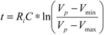
where Vp is the unloaded battery voltage.
Since Vp is unknown it must be estimated. It should be chosen to match the end-of-life unloaded battery voltage, and from these measurements a value of 2,7 V looks like a good starting point. With this, the example yielded:
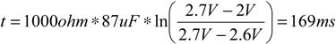
Since t is shorter than the sleep state time, this looks like a good sized capacitor.
If t is longer than the sleep state, either Vmax or Ri need to be reduced. If t is considerably shorter than the sleep state, the capacitor is unnecessarily large and can be reduced by increasing Vmax (alternatively if C is left unchanged the circuit will be able to handle a higher Ri).
Note that in the test load profile, the sleep current was a non-negligible 100 μA. This called for a slightly larger capacitor of 100 μF instead of the 87 μF calculated above.
For more information contact Stuart Hanford, Arrow Altech Distribution, +27 (0)11 923 9600, [email protected], www.arrow.altech.co.za
| Tel: | +27 11 923 9600 |
| Email: | [email protected] |
| www: | www.altronarrow.com |
| Articles: | More information and articles about Altron Arrow |


© Technews Publishing (Pty) Ltd | All Rights Reserved
 printer friendly version