


Smartphones, tablets, digital cameras, navigation systems, medical equipment and other low-power portable devices often contain multiple integrated circuits manufactured on different semiconductor processes. These devices typically require several independent supply voltages, each usually different than the voltage supplied by the battery or external AC-to-DC power supply.
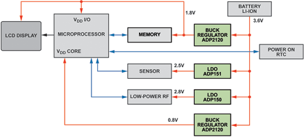
Figure 1 shows a typical low-power system operating with a Li-Ion battery. The battery’s usable output varies from 3 V to 4,2 V, while the ICs require 0,8 V, 1,8 V, 2,5 V and 2,8 V. A simple way to reduce the battery voltage to a lower DC voltage is to use a low dropout regulator (LDO). Unfortunately, power not delivered to the load is lost as heat, making LDOs inefficient when VIN is much greater than VOUT.
A popular alternative, the switching converter, alternately stores energy in an inductor’s magnetic field and releases the energy to the load at a different voltage. Its reduced losses make it a better choice for high efficiency. Buck, or step-down, converters provide lower voltage. Boost, or step-up, converters provide higher output voltage. Switching converters that include internal FETs as switches are called switching regulators, while devices requiring external FETs are called switching controllers. Most low-power systems use both LDOs and switching converters to achieve cost and performance objectives.
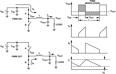
Buck regulators consist of two switches, two capacitors and an inductor, as shown in Figure 2. Non-overlapping switch drives ensure that only one switch is on at a time to avoid unwanted current shoot-through. In phase 1, switch B is open and switch A is closed. The inductor is connected to VIN, so current flows from VIN to the load. The current increases due to the positive voltage across the inductor.
In phase 2, switch A is open and switch B is closed. The inductor is connected to ground, so current flows from ground to the load. The current decreases due to the negative voltage across the inductor, and energy stored in the inductor is discharged into the load.
Note that the switching regulator operation can be continuous or discontinuous. When operating in continuous conduction mode (CCM), the inductor current never drops to zero; when operating in discontinuous conduction mode (DCM), the inductor current can drop to zero. Low-power buck converters rarely operate in DCM. The current ripple, shown as ΔIL in Figure 2, is typically designed to be 20% to 50% of the nominal load current.
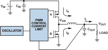
In Figure 3, switch A and switch B have been implemented with PFET and NFET switches, respectively, to create a synchronous buck regulator. The term synchronous indicates that a FET is used as the lower switch. Buck regulators that use a Schottky diode in place of the lower switch are defined as asynchronous (or non-synchronous).
For handling low power, synchronous buck regulators are more efficient because the FET has a lower voltage drop than a Schottky diode. However, the synchronous converter’s efficiency at light load will be compromised if the bottom FET is not released when the inductor current reaches zero, and additional control circuitry increases the complexity and cost of the IC.
Today’s low-power synchronous buck regulators use pulse-width modulation (PWM) as the primary operating mode. PWM holds the frequency constant and varies the pulse width (tON) to adjust the output voltage. The average power delivered is proportional to the duty cycle, D, making this an efficient way to provide power to a load.
The FET switches are controlled by a pulse-width controller, which uses either voltage- or current feedback in a control loop to regulate the output voltage in response to load changes. Low-power buck converters generally operate between 1 MHz and 6 MHz. Higher switching frequencies allow the use of smaller inductors, but efficiency is decreased by approximately 2% for every doubling of the switching frequency.
PWM operation does not always improve system efficiency at light loads. Consider, for example, the power circuitry for a graphics card. As the video content changes, so does the load current on the buck converter driving the graphics processor. Continuous PWM operation can handle a wide range of load currents, but the efficiency rapidly degrades at light loads because the power required by the regulator consumes a larger percentage of the total power delivered to the load. For portable applications, buck regulators incorporate additional power-saving techniques, such as pulse-frequency modulation (PFM), pulse skipping or a combination of both.
Analog Devices defines efficient light-load operation as power-save mode (PSM). When the power-save mode is entered, an offset induced in the PWM regulation level causes the output voltage to rise, until it reaches approximately 1,5% above the PWM regulation level, at which point PWM operation turns off: both power switches are off, and idle mode is entered. COUT is allowed to discharge until VOUT falls to the PWM regulation voltage. The device then drives the inductor, causing VOUT to again rise to the upper threshold. This process is repeated as long as the load current is below the power-save current threshold.
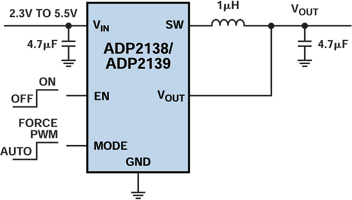
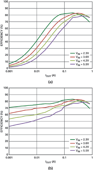
The ADP2138 is a compact 800 mA, 3 MHz step-down DC-to-DC converter. Figure 4 shows a typical applications circuit. Figure 5 shows the improvement in efficiency between forced PWM and automatic PWM/PSM operation. Due to the variable frequency, PSM interference can be hard to filter, so many buck regulators include a MODE pin (shown in Figure 4) that allows the user to force continuous PWM operation or allow automatic PWM/PSM operation. The MODE pin can be hardwired for either operating mode or dynamically switched when needed to save power.
Buck regulators improve efficiency
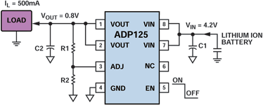
Increased efficiency allows longer battery operating times before replacement or recharging, a highly desirable feature in new portable device designs. For example, a rechargeable Li-Ion battery can drive a 500 mA load at 0,8 V using the ADP125 LDO, as shown in Figure 6. The LDO’s efficiency, VOUT/VIN × 100%, or 0,8/4,2, is only 19%. LDOs cannot store the unused energy, so the 81% (1,7 W) of power not delivered to the load is dissipated as heat within the LDO, which could cause a handheld device to heat up quickly.
Using the ADP2138 switching regulator, which offers 82% operating efficiency with a 4,2 V input and 0,8 V output, delivers more than four times the efficiency and reduces the temperature rise of the portable device. Such substantial improvements in system efficiency have resulted in large numbers of switching regulators being designed into portable devices.
Key buck converter specifications and definitions
Input voltage range: A buck converter’s input voltage range determines the lowest usable input supply voltage. The specifications may show a wide input voltage range, but VIN must be greater than VOUT for efficient operation. For example, a regulated 3,3 V output voltage requires an input voltage above 3,8 V.
Ground or quiescent current: IQ is the DC bias current not delivered to the load. Devices with lower IQ provide higher efficiency. IQ can be specified for many conditions, however, including switching off, zero load, PFM operation or PWM operation, so it is best to look at actual operating efficiency data at specific operating voltages and load currents to determine the best buck regulator for an application.
Shutdown current: This is the input current consumed when the enable pin has been set to off. This current, usually well below 1 μA for low-power buck regulators, is important during long standby times on the battery while the portable device is in sleep mode.
Output voltage accuracy: Analog Devices buck converters are designed for high output voltage accuracy. Fixed-output devices are factory trimmed to better than ±2% at 25°C. Output voltage accuracy is specified over the operating temperature, input voltage, and load current ranges, with worst-case inaccuracies specified as ±x%.
Line regulation: Line regulation is the change in output voltage caused by a change in the input voltage, at the rated load.
Load regulation: Load regulation is the change of the output voltage for a change in the output current. Most buck regulators can hold the output voltage essentially constant for slowly changing load current.
Load transients: Transient errors can occur when the load current quickly changes from low to high, causing mode switching between PFM and PWM or from PWM to PFM operation. Load transients are not always specified, but most data sheets have plots of load transient responses at different operating conditions.
Current limit: Buck regulators such as the ADP2138 incorporate protection circuitry to limit the amount of positive current flowing through the PFET switch and the synchronous rectifier. The positive current control limits the amount of current that can flow from the input to the output. The negative current limit prevents the inductor current from reversing direction and flowing out of the load.
Soft start: It is important for buck regulators to have an internal soft-start function that ramps the output voltage in a controlled manner upon startup to limit the inrush current. This prevents input voltage from a battery or high-impedance power source from dropping when it is connected to the input of the converter. After the device is enabled, the internal circuit begins the power-up cycle.
Startup time: Startup time is the time between the rising edge of the enable signal and when VOUT reaches 90% of its nominal value. This test is usually performed with VIN applied and the enable pin toggled from off to on. In cases where the enable is connected to VIN, when VIN is toggled from off to on, the startup time can substantially increase because the control loop takes time to stabilise. Startup time of a buck regulator is important for applications where the regulator is frequently turned on and off to save power in portable systems.
Thermal shutdown (TSD): If the junction temperature rises above the specified limit, the thermal shutdown circuit turns the regulator off. Extreme junction temperatures can be the result of high-current operation, poor circuit board cooling or high ambient temperature. Hysteresis is included in the protection circuit to prevent return to normal operation until the on-chip temperature drops below the preset limit.
100% duty cycle operation: With a drop in VIN or an increase in ILOAD, the buck regulator reaches a limit where the PFET switch is on 100% of the time and VOUT drops below the desired output voltage. At this limit, the ADP2138 smoothly transitions to a mode where the PFET switch stays on 100% of the time. When the input conditions change, the device immediately restarts PWM regulation with no overshoot of VOUT.
Discharge switch: In some systems, if the load is very light, a buck regulator’s output can stay high for some time after the system enters sleep mode. Then, if the system starts the power-on sequence before the output voltage has discharged, the system may latch up, or devices can be damaged. The ADP2139 buck regulator uses an integrated switched resistor (typically 100 Ω) to discharge the output when the enable pin goes low or when the device enters under-voltage lockout or thermal shutdown.
Under-voltage lockout: Under-voltage lockout (UVLO) ensures that voltage is supplied to the load only when the system input voltage is above the specified threshold. UVLO is important because it allows the device to power on only when the input voltage is at or above the value required for stable operation.
| Tel: | +27 11 923 9600 |
| Email: | [email protected] |
| www: | www.altronarrow.com |
| Articles: | More information and articles about Altron Arrow |


© Technews Publishing (Pty) Ltd | All Rights Reserved
 printer friendly version