


Chip designers often find themselves in a situation where the board layout has been completed before the chip is designed. The FPGA they are targeting must satisfy an external input phase relationship - usually between clock and data inputs. In this article, Actel shows how maintaining this phase relationship for signals going off-chip enables them to meet external set-up and hold requirements.
There are special delay macros called BUFD and INVD that give designers more control in the timing behaviour of their designs. BUFD is a special version of the buffer (BUFF), which will not be removed by Actel's Designer Software in its optimisation steps. This macro will always be retained and its delay preserved after the compile and layout steps. Similarly, INVD is a special version of the inverter (INV), which is preserved after compilation and layout.
The suggested uses of BUFD and INVD are as follows:
* Maintain the phase relationship between clock and data input signals when sending signals derived from these signals off-chip. This application enables them to meet external set-up and hold requirements.
* Maintain the phase relationship of clock and data input signals in designs with high-fanout clock signals.
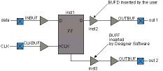
As shown in Figure 1, a certain phase relationship exists between the clock and data signals (generally, the data signal lags the clock signal). Employing BUFD is recommended to maintain this phase relationship. All the antifuse device families from Actel have a restriction that a CLKBUF cannot be connected directly to an OUTBUF, so Designer Software will automatically insert a BUFF module (inst3 in Figure 1). This will introduce a delay that may cause the data signal to arrive ahead of the sys_clk signal going off-chip.
To prevent this, the user can insert a BUFD macro in his netlist. The BUFD, unlike a regular BUFF, is assigned the ALSPRESERVE property. This ensures that the BUFD will not be optimised away during the compilation step and hence can offset the delay caused by automatic insertion of the BUFF in the sys_clk path. This technique maintains the phase relationship of the data and clock inputs when going off-chip and the external set-up and hold requirements can be met.
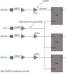
In Figure 2, the clock signal coming from the CLKBUF has a high fanout. This means increased capacitive loading and hence increased delay. In contrast, the data signal has a fanout of only one. The clock network's high fanout may allow the data input to (undesirably) lead the clock signal. Again, introducing one or more BUFD macros (inst1) in the data signal path provides enough delay to offset the delay of the high-fanout clock net. If inversion of the signal is required in addition to delay, the INVD macro is available. Again, the ALSPRESERVE property is assigned to this macro to avoid elimination during optimisation steps.
For further information contact Kobus van Rooyen, ASIC Design Services, (011) 315 8316, [email protected]
| Tel: | +27 11 315 8316 |
| Email: | [email protected] |
| www: | www.asic.co.za |
| Articles: | More information and articles about ASIC Design Services |


© Technews Publishing (Pty) Ltd | All Rights Reserved
 printer friendly version