


A key requirement across a multitude of industries is to accurately produce, easily manipulate and quickly change waveforms of various frequencies and types.
Whether a wideband transceiver requires an agile low-phase-noise frequency source with excellent spurious-free dynamic performance or an industrial measurement and control system needs a stable frequency stimulus, the ability to quickly, easily and cost effectively generate an adjustable waveform while maintaining phase continuity is a critical design criterion that direct digital frequency synthesis can fulfil.
The task of frequency synthesis
Increasing spectrum congestion, coupled with the insatiable need for lower-power, higher-quality measurement equipment, calls for the use of new frequency ranges and better exploitation of existing ones. As a result, better control of frequency generation is being sought – in most cases with the assistance of frequency synthesisers.
These devices use a given frequency, fC, to generate a waveform at a related desired frequency (and phase), fOUT. The general relationship can be written simply as fOUT = εx × fC where the scaling factor, εx, is sometimes called the normalised frequency.
The equation is always implemented using algorithms for step-by-step approximations of real numbers. When the scaling factor is a rational number, a ratio of two relatively prime integers, the output frequency and the reference frequency will be harmonically related. In most cases, however, εx can belong to a much broader set of real numbers, and the approximation process is truncated as soon as it falls within an acceptable limit.
Direct digital frequency synthesis
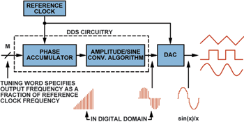
One such practical realisation of a frequency synthesiser is direct digital frequency synthesis (DDFS), often shortened to direct digital synthesis (DDS). The technique uses digital data processing to generate a frequency- and phase-tuneable output related to a fixed frequency reference, or clock source, fC. In a DDS architecture, the reference or system clock frequency is divided down by the scaling factor, set by a programmable binary tuning word.
Simply stated, a direct digital frequency synthesiser translates a train of clock pulses into an analog waveform, typically a sine, triangular or square wave. As Figure 1 shows, its essential parts are: a phase accumulator, which produces a number corresponding to a phase angle of the output waveform; a phase-to-digital converter, which generates the instantaneous digital fraction of the output amplitude occurring at a particular phase angle; and a digital-to-analog converter (DAC), which converts that digital value to a sampled analog data point.
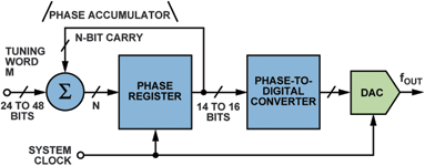
For sine-wave outputs, the phase-to-digital converter is usually a sine lookup table (Figure 2). The phase accumulator counts by N, to generate a frequency related to fC according to the equation:

Where M is the resolution of the tuning word (24 bits to 48 bits) and N is the number of pulses of fC corresponding to the smallest incremental phase change of the phase accumulator’s output word.
Since changes to N result in immediate changes in the output phase and frequency, the system is inherently phase-continuous, a critical attribute in many applications. No loop settling time is required, in contrast to analog-type systems such as phase-locked loops (PLLs).
The DAC is usually a high-performance circuit specifically designed to work with the DDS core (phase accumulator and phase-to-amplitude converter). In most cases, the resulting device, often a single chip, is commonly referred to as a complete DDS or C-DDS.
Practical DDS devices often integrate multiple registers to allow various frequency – and phase-modulation schemes to be realised. When included, the phase register’s contents are added after the phase accumulator. This enables the output sine wave to be phase-delayed in correspondence with a phase tuning word.
This is extremely useful for phase-modulation applications in communication systems. The resolution of the adder circuit determines the number of bits in the phase tuning word and, therefore, the resolution of the delay.
Integrating a DDS engine and a DAC in a single device has advantages and disadvantages, but whether integrated or not, a DAC is required to create a high-quality analog signal of exceptional purity.
The DAC converts the digital sine output into an analog sine wave and may be either single-ended or differential. A few of the key requirements are low phase noise, excellent wideband (WB) and narrow-band (NB) spurious-free dynamic range (SFDR) and low power consumption. If it is an external component, the DAC needs to be fast enough to process the signal, so devices with a parallel port are common.
DDS vs. other solutions
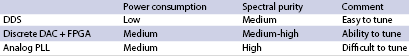
Other possibilities for frequency generation include analog phase-locked loops (PLLs), clock generators, and using an FPGA to dynamically program the output of a DAC. A simple comparison of the technologies can be made by examining spectral performance and power consumption, qualitatively demonstrated in Table 1.
A phase-locked loop is a feedback loop comprising a phase comparator, a divider and a voltage-controlled oscillator (VCO). The phase comparator compares a reference frequency with the output frequency (usually divided down by a factor, N). The error voltage generated by the phase comparator is applied to the VCO, which generates the output frequency. When the loop has settled, the output will bear an accurate relationship to the reference in frequency and/or phase.
PLLs have long been recognised as superior devices for low phase noise and high spurious-free dynamic range (SFDR) applications requiring high fidelity and stable signals in a specific band of interest. Their inability to accurately and quickly tune the frequency output and waveform and their slow response limits their suitability for applications such as agile frequency hopping and some frequency – and phase-shift keying applications.
Other approaches, including field-programmable gate arrays (FPGAs) with embedded DDS engines – in combination with off-the-shelf DACs to synthesise output sine waves – solve the frequency-hopping difficulties of PLLs, but have their own weaknesses.
The main system disadvantages include higher operating and interface power requirements, higher cost, large size and additional software-, hardware- and memory overhead for the system developer. For example, up to 72 KB of memory are required to generate a 10 MHz output signal with 60 dB dynamic range using the DDS engine option on modern FPGAs. In addition, the designer needs to be comfortable and familiar with subtle trade-offs and the architecture of the DDS core.
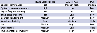
As a practical matter (see Table 2), rapid advances in CMOS processing, together with modern digital design techniques and improved DAC topologies, have resulted in DDS technology achieving power consumption, spectral performance and cost levels that were previously unattainable for a wide range of applications.
While complete DDS products will never match the highest performance and design flexibility achievable with custom combinations of high-end DAC technology and FPGAs, the size, power and cost benefits, coupled with the simplicity of DDS devices, may make them easily the first choice for many applications.
Also note that since a DDS device fundamentally embodies a digital method of generating an output waveform, it can simplify the architecture of some solutions or make it possible to digitally program the waveform.
While a sine wave is normally used to explain the function and operation of a DDS, it is easily possible to generate triangular or square (clock) wave outputs from modern DDS ICs, avoiding the need for a lookup table in the former case, and for a DAC in the latter case, where the integration of a simple yet precise comparator will suffice.
The next part of this article, covering DDS performance and limitations as well as applications, will run in a future issue of Dataweek.


© Technews Publishing (Pty) Ltd | All Rights Reserved
 printer friendly version