


Part 1 of this article appeared in the 17 April issue.
DDS performance and limitations
Images and envelopes: sin(x)/x roll-off
The actual output of the DAC is not a continuous sine wave but a train of pulses with a sinusoidal time envelope. The corresponding frequency spectrum is a set of images and aliases. The images lie along a sin(x)/x envelope (see |amplitude| plot in Figure 3). Filtering is necessary to suppress frequencies outside the band of interest, but it cannot suppress higher-order aliases (due to DAC non-linearities, for example) appearing within the pass band.
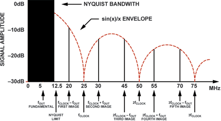
The Nyquist criterion dictates that a minimum of two samples per cycle are required to reconstruct a desired output waveform. Image responses are created in the sampled output spectrum at K fCLOCK ± fOUT. In this example, where fCLOCK = 25 MHz and fOUT = 5 MHz, the first and second images occur (see Figure 3) at fCLOCK ± fOUT, or 20 MHz and 30 MHz. The third and fourth images appear at 45 MHz and 55 MHz.
Note that the sin(x)/x nulls appear at multiples of the sampling frequency. In the case where fOUT is greater than the Nyquist bandwidth (½ fCLOCK), the first image response will appear within the Nyquist bandwidth as an aliased image (a 15 MHz signal will alias down to 10 MHz, for example). The aliased image cannot be filtered from the output with a traditional Nyquist antialiasing filter.
In typical DDS applications, a low-pass filter is utilised to suppress the effects of the image responses in the output spectrum. To keep the cutoff requirements of the low-pass filter reasonable and the filter design simple, an accepted guideline is to limit the fOUT bandwidth to approximately 40% of the fCLOCK frequency using an economical low-pass output filter.
The amplitude of any given image in response to the fundamental can be calculated using the sin(x)/x formula. Because the function rolls off with frequency, the amplitude of the fundamental output will decrease inversely with its tuned frequency; in a DDS system, the decrease will be –3,92 dB over the DC to Nyquist bandwidth.
The amplitude of the first image is substantial – within 3 dB of the fundamental. To simplify filtering requirements for DDS applications, it is important to generate a frequency plan and analyse the spectral considerations of the image and the sin(x)/x amplitude responses at the desired fOUT and fCLOCK frequencies.
Online interactive design tools supporting the Analog Devices DDS product family allow for quick and easy simulation of where images lie and allow the user to choose frequencies where images are outside the band of interest.
Other anomalies in the output spectrum, such as integral and differential linearity errors of the DAC, glitch energy associated with the DAC, and clock feed-through noise, will not follow the sin(x)/x roll-off response. These anomalies will appear as harmonics and spurious energy in many places in the output spectrum, but will generally be much lower in amplitude than the image responses.
The general noise floor of a DDS device is determined by the cumulative combination of substrate noise, thermal noise effects, ground coupling and other sources of signal coupling. The noise floor, performance spurs and jitter of a DDS device are greatly influenced by circuit board layout, the quality of the power supplies and – most importantly – the quality of the input reference clock.
Jitter
A perfect clock source would have edges occurring at precise intervals in time that would never vary. This, of course, is impossible; even the best oscillators are constructed from non-ideal components and have noise and other imperfections. A high-quality, low-phase-noise crystal oscillator will have jitter on the order of picoseconds, accumulated over many millions of clock edges.
Jitter is caused by thermal noise, instabilities in the oscillator’s electronic circuitry, and external interference through the power, ground and output connections – all contributing to disturbances in the oscillator’s timing. In addition, oscillators are influenced by external magnetic or electric fields, and RF interference from nearby transmitters. A simple amplifier, inverter or buffer in the oscillator circuitry will also add jitter to a signal.
So choosing a stable reference clock oscillator with low jitter and sharp edges is critical. Higher-frequency reference clocks allow greater oversampling, and jitter can be somewhat ameliorated by frequency division, since dividing the frequency of the signal yields the same amount of jitter across a longer period, and so reduces the percentage of jitter on the signal.
Noise – including phase noise
Noise in a sampled system depends on many factors, starting with reference clock jitter, which shows up as phase noise on the fundamental signal. In a DDS system, truncation of the phase register output may introduce code-dependent system errors.
Binary-coded words do not cause truncation errors. For non-binary coded words, however, the phase-noise truncation error produces spurs in the spectrum. The frequency/magnitude of the spurs is determined by the code word. The DAC’s quantisation and linearity errors will also add harmonic noise in the system. Time domain errors, such as undershoot/overshoot and code glitches, all contribute distortion to the output signal.
Applications
DDS applications can be segmented into two primary categories:
Communication and radar systems that require agile frequency sources for data encoding and modulation applications.
Measurement, industrial and optical applications that require a generic frequency synthesis function with programmable tuning, sweeping and excitation.
In both cases, an increasing trend towards higher spectral purity (lower phase noise and higher spurious-free dynamic range) is coupled with low operating power and size requirements for remote or battery-operated equipment.
DDS in modulation/data encoding and synchronisation
From its exclusive origins in radar and military applications, some of the advances in DDS product characteristics (performance improvements, cost and size) have combined to make DDS technology very popular in modulation and data encoding applications. This section will discuss two data encoding schemes and their proposed implementation with a DDS system.
Binary frequency shift keying (BFSK, or simply FSK) is one of the simplest forms of data encoding. The data is transmitted by shifting the frequency of a continuous carrier between one (binary 1, or mark) and the other (binary 0, or space) of two discrete frequencies. Figure 4 shows the relationship between the data and the transmitted signal.
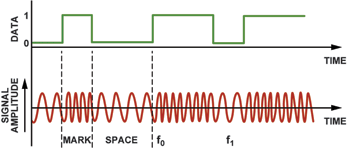
Binary 1s and 0s are represented as two different frequencies – f0 and f1, respectively. This encoding scheme is easily implemented with a DDS device. The DDS frequency tuning word representing the output frequencies is changed so that f0 and f1are generated from 1s and 0s to be transmitted.
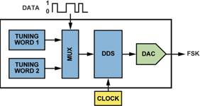
In at least two members of Analog Devices’ complete DDS product families (the AD9834 and the AD9838), the user can simply program the two current FSK frequency tuning words into the IC’s embedded frequency registers. To shift output frequency, a dedicated pin selects the register containing the appropriate tuning word (see Figure 5).
Phase-shift keying (PSK) is another simple form of data encoding. In PSK, the frequency of the carrier remains constant, and the phase of the transmitted signal is varied to convey the information.
Several schemes can be used to accomplish PSK. The simplest method, commonly known as binary PSK (or BPSK), uses only two signal phases: 0° (Logic 1) and 180° (Logic 0). The state of each bit is determined according to the state of the preceding bit.
If the phase of the wave does not change, the signal state stays the same (low or high). If the phase of the wave changes by 180°, that is, if the phase reverses – the signal state changes (low to high, or high to low).
PSK encoding is easily implemented with a DDS product as most of the devices have a separate input register (a phase register) that can be loaded with a phase value. This value is directly added to the phase of the carrier without changing its frequency. Changing the contents of this register modulates the phase of the carrier, generating a PSK output.
For applications that require high-speed modulation, the AD9834 and AD9838, which have pairs of phase registers, allow signals on a PSELECT pin to alternate between the preloaded phase registers to modulate the carrier as required.
More complex forms of PSK employ four or eight wave phases. This allows binary data to be transmitted at a faster rate per phase change than is possible with BPSK modulation. In four-phase modulation (quadrature PSK), the possible phase angles are 0°, +90°, -90° and +180°; each phase shift can represent two signal elements.
The AD9830, AD9831, AD9832 and AD9835 provide four phase registers to allow complex phase modulation schemes to be implemented by continuously updating different phase offsets to the registers.
I/Q capability using multiple DDS components in synchronous mode
Many applications require the generation of two or more sinusoidal or square wave signals having a known phase relationship. A popular example is in-phase and quadrature modulation (I/Q), a technique wherein signal information is derived from a carrier frequency at its 0° and 90° phase angles.
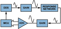
Two single DDS components can be run from the same source clock to output signals whose phase relationship can be directly controlled and manipulated. In Figure 6, the AD9838 devices are programmed using one reference clock; the same RESET pin is used to update both devices. In this way, simple I/Q modulation can be achieved.
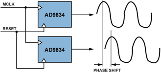
A reset must be initiated after power-up and before transferring any data to the DDS. This establishes the DDS output in a known phase, which becomes the common reference angle that allows synchronisation of multiple DDS devices.
When new data is sent simultaneously to multiple DDS devices, a coherent phase relationship can be maintained – or the relative phase offset between multiple DDS devices can be predictably shifted by means of the phase offset register. The AD983x series of DDS products have 12 bits of phase resolution, providing an effective resolution of 0,1°.
Network analysis
Many applications in the electronic world involve the gathering and decoding of data from networks such as analog measurement and optical communications systems. Normally, the system analysis requirement is to stimulate a circuit or system with a frequency of known amplitude and phase, and analyse the signal characteristics of the response signal through the system.
The information gathered on the response signal is used to determine key system information. The range of networks being tested (see Figure 7) can be quite wide, including cable integrity testing, biomedical sensing and flow-rate measurement systems.
Wherever the basic requirement is to generate frequency-based signals and compare phase and amplitude of the response signal(s) to the original signal, or if a range of frequencies needs to be excited through the system, or if test signals with different phase relationships (as in systems with I/Q capability) are required, direct digital synthesis ICs can be highly useful for digitally controlling stimulus frequency and phase through software with simplicity and elegance.
Cable integrity/loss measurement
Cable integrity measurement is a non-invasive method of analysing cables in applications such as airplane wiring, local area networks (LANs) and telephone lines.
One way to determine performance is to see how much signal is lost through the cable. By injecting a signal of known frequency and amplitude, the user can calculate cable attenuation by measuring the amplitude and phase at remote portions of the cable.
Parameters such as DC resistance and characteristic impedance will affect a particular cable’s attenuation. The result is usually expressed in decibels below the signal source (0 dB) over the frequency range of the test. The frequencies of interest depend on the cable type. DDS devices, with their ability to generate a wide range of frequencies, can be used as a stimulus with the necessary frequency resolution.
Flow meter
A related application area is in water, other liquids, and gas flow analysis in pipelines. An example is ultrasonic flow measurement, which operates on a phase-shift principle, as shown in Figure 8.
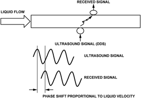
Basically, a signal is transmitted from one side of the channel where the liquid is flowing and a transducer sensor is positioned on the opposite side to measure the phase response, which depends on the flow rate. There are many variations on this technique. Test frequencies depend on the substance being measured; in general, the output signal is often transmitted over a range of frequencies. DDS provides the flexibility to set and change the frequency seamlessly.


© Technews Publishing (Pty) Ltd | All Rights Reserved
 printer friendly version