


The overall precision of a high-resolution, successive approximation analog-to-digital converter (ADC) depends on the accuracy, stability and drive capability of its voltage reference. The switched capacitors on the ADC’s reference input present a dynamic load, so the reference circuit must be able to handle time- and throughput-dependent currents.
Some ADCs integrate the reference and reference buffer on chip, but these may not be optimal in terms of power or performance - and the best performance can usually be achieved with an external reference circuit. This article looks at the challenges and requirements involved with the reference circuit design.
Reference input
A simplified schematic of a successive approximation ADC is shown in Figure 1.
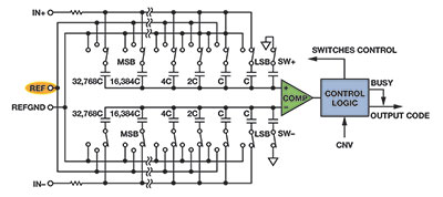
During the sampling interval, the capacitive digital-to-analog converter (DAC) is connected to the ADC input, and a charge proportional to the input voltage is stored in its capacitors. When the conversion starts, the DAC is disconnected from the input.
The conversion algorithm successively switches each bit to the reference or ground. Charge redistribution on the capacitors causes current to be drawn from or sunk by the reference. This dynamic current load is a function of both the ADC throughput rate and the internal clock that controls the bit trials. The most significant bits (MSBs) hold the most charge and require the most current.
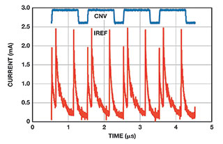
Figure 2 shows the dynamic current load on the reference input of the AD7980, a 16-bit, 1 MSps, PulSAR successive approximation ADC. The measurement was made by observing the voltage drop across a 500 Ω resistor placed between the reference source and the reference pin. The plot shows current spikes of up to 2,5 mA, along with smaller spikes spread over the conversion.
To supply this current, while keeping the reference voltage free of noise, a high value, low ESR reservoir capacitor, typically 10 µF or more, should be placed as close as possible to the reference input. A larger capacitor will further smooth the current load and reduce the burden on the reference circuit, but stability becomes an issue with very large capacitors.
The reference must be capable of supplying the average current needed to top up the reference capacitor without causing the reference voltage to droop significantly. In ADC data sheets, the average reference input current is typically specified at a particular throughput rate.
For example, the AD7980 data sheet specifies the average reference current to be 330 µA typical at 1 MSps with a 5 V reference. No current is drawn between conversions, so the reference current scales linearly with throughput, dropping to 33 µA at 100 KSps.
The reference (or reference buffer) must have low enough output impedance at the highest frequency of interest to maintain the voltage at the ADC input without a significant current-induced voltage drop.
Reference output drive
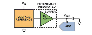
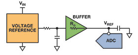
Figure 3 shows a typical reference circuit. The voltage reference may integrate a buffer that has sufficient drive current, or a suitable op-amp can be used as a buffer. To avoid conversion errors, the average current required at a particular throughput should not cause the reference voltage to droop more than ½ LSB. This error will be most pronounced during a burst conversion, as the reference load will go from zero to the average reference current at that throughput.
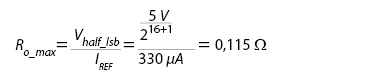
Using the AD7980 16-bit ADC with IREF = 330 µA and VREF = 5 V as an example to determine whether a reference has sufficient drive capability, the maximum allowed output impedance for a ½ LSB voltage drop is:
Most voltage references don’t specify output impedance, but they do specify load regulation, usually in ppm/mA. To convert to output impedance, multiply by the reference voltage and divide by 1000. For example, the ADR435 ultra-low-noise XFET 5 V reference specifies load regulation of 15 ppm/mA maximum when sourcing current. Converting to ohms gives:
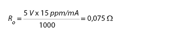
So, the ADR435 should be suitable from an output impedance perspective. It can source up to 10 mA, which is more than enough to handle the 330 µA average reference current.
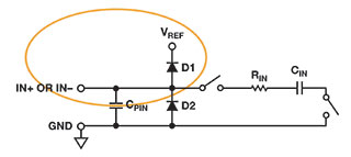
When the ADC input voltage exceeds the reference voltage, even momentarily, it can inject current into the reference, so the reference must also be able to sink some current. Figure 4 shows the diode connection between the ADC and reference inputs that can cause current flow into the reference during an input over-range condition. Unlike some older references, the ADR435 can sink 10 mA.
As the reference current requirement scales linearly with throughput, a higher output impedance (lower power) reference may be acceptable at lower throughput rates, or when using ADCs with lower throughput, such as the 500 KSps AD7988-5 or 100 KSps AD7988-1 (IREF = 250 µA).
The maximum output impedance can be calculated with the reduced reference current. Note that these equations should only be used as guidelines, and the selected reference should be tested for drive capability in hardware.
A reference buffer can be used when the drive of the chosen reference is insufficient, or when a micropower reference is preferred. This can be implemented with a suitable op-amp in a unity-gain configuration. The op-amp must have low noise and suitable output drive capability, and it must be stable with a large capacitive load. It must also be able to supply the necessary current.
Op-amp output impedance is not generally specified but can often be determined from output impedance vs. frequency plots, as shown in Figure 5 for the AD8031 80 MHz rail-to-rail op-amp.
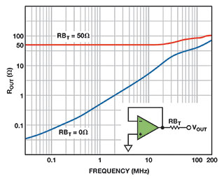
The output impedance is less than 0,1 Ω below 100 kHz and less than 0,05 Ω at DC, so this is a good choice in terms of output drive for the example of driving the AD7980 at 1 MSps. Maintaining low output impedance over a wide frequency range is important for driving the reference input.
The reservoir capacitor will never completely smooth out the current draw at the reference input, even with a large capacitor. The frequency content of the current ripple will be a function of the throughput and the input signal bandwidth.
The large reservoir capacitor handles the high-frequency, throughput-dependent current while the reference buffer must be able to maintain low impedance up to the maximum input signal frequency – or to a frequency where the reservoir capacitor impedance becomes low enough to supply the necessary current. Typical plots in reference data sheets show output impedance vs. frequency and should be taken into consideration when choosing the reference.
The AD8031 is a good choice, as it is stable with capacitive loads greater than 10 µF. Other op-amps, such as the ADA4841, will also be stable with large capacitors, as they mainly have to drive a stable DC level, but particular op-amps must be tested to determine their behaviour when loaded. It is not a good idea to use a series resistor before the capacitor to maintain stability, as this will increase the output impedance.
A reference buffer is very useful for driving multiple ADCs from one reference, as is the case in simultaneous-sampling applications, such as that shown in Figure 6.
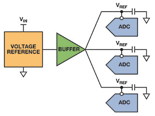
Each ADC reference input has its own reservoir capacitor placed as close as possible to the reference input pin. The trace from each reference input is routed back to a star connection at the output of the reference buffer to minimise crosstalk effects.
Reference buffers that have low output impedance and high output current capability can drive many ADCs, depending on their current requirements. Note that the buffer must also be stable with the extra capacitance associated with multiple reference capacitors.
Noise and temperature drift
Once the drive capability has been determined, it must be ensured that the noise from the reference circuit does not affect the ADC’s performance. To preserve the signal-to-noise ratio (SNR) and other specifications, the noise contribution from the reference must be kept to a fraction (ideally 20% or less) of the ADC noise.
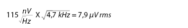
The AD7980 specifies 91 dB SNR with a 5 V reference. Converting to rms gives:
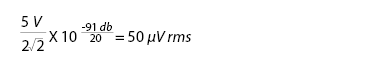
Thus, the reference circuit should have less than 10 µV rms noise to have minimal impact on the SNR. The noise specification for references and op amps is typically split into two parts: low-frequency (1/f) noise and wideband noise. Combining the two will give the total noise contribution of the reference circuit. Figure 7 shows a typical noise vs. frequency plot for the ADR431 2,5 V reference.
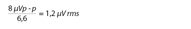
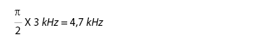
The ADR435 compensates its internal op-amp to drive large capacitive loads and avoid noise peaking, making it very attractive for use with ADCs. This is explained in greater detail in the data sheet. With a 10 µF capacitor, it specifies 8 µV p-p 1/f (0,1 Hz to 10 Hz) noise and 115 nV/√Hz wideband noise spectral density. The estimated noise bandwidth is 3 kHz.
To convert the 1/f noise from peak-to-peak to rms, divide by 6,6 to get:
Next, calculate the wideband noise contribution using the estimated bandwidth with a 10 µF capacitor. The effective bandwidth will be given by:
Use this effective bandwidth to calculate the rms wideband noise:
The total rms noise is the root sum square of the low-frequency noise and the wideband noise:
This is less than 10 µV rms, so it won’t significantly impact the ADC’s SNR. These calculations can be used to estimate the noise contribution of the reference to determine its suitability, but this will need to be verified on the bench with real hardware.
The same analysis can be used to calculate the noise contribution if a buffer is used after the reference. The AD8031, for example, has 15 nV/√Hz noise spectral density. With a 10 µF capacitor on its output, its measured bandwidth is reduced to about 16 kHz. Using this bandwidth and noise density, and ignoring the 1/f noise, the noise contribution will be 2,4 µV rms.
The reference buffer noise can be root sum squared with the reference noise to arrive at a total noise estimate. Generally the reference buffer should have a noise density much less than that of the reference.
When using a reference buffer, it is possible to band limit the noise from the reference even further by adding an RC filter with a very low cutoff frequency to the output of the reference, as shown in Figure 8. This can be useful, considering the reference is usually the dominant source of noise.
Some other important considerations for choosing a reference are initial accuracy and temperature drift. The initial accuracy is specified in percent or mV. Many systems allow for calibration, so initial accuracy is not as important as drift, which is typically specified in ppm/°C or µV/°C. Most good references have less than 10 ppm/°C drift, and the ADR45xx family drives drift down to a couple of ppm/°C. This drift must be incorporated into the system’s error budget.
Troubleshooting reference issues
A poorly designed reference circuit can cause serious conversion errors. The most common manifestation of a reference issue is repeated or ‘stuck’ codes from the ADC. This happens when noise on the reference input is large enough to cause the ADC to make an incorrect bit decision.
This may show up as the same code being repeated many times, even though the input is changing, or a repeated string of ones or zeros in the less significant bits, as shown in Figure 9. The areas circled in red show where the ADC gets stuck, repeatedly returning the same code.
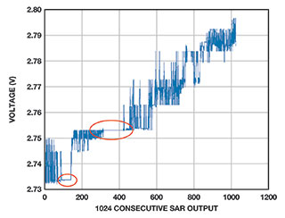
The problem generally gets worse near full scale because the reference noise has a greater impact on the more significant bit decisions. Once an incorrect bit decision has been made, the remaining bits become filled with ones or zeros. The most common reasons for these ‘stuck’ bits are the size and placement of the reference capacitor, insufficient drive strength of the reference/reference buffer, or poor selection of the reference/reference buffer, resulting in excess noise.
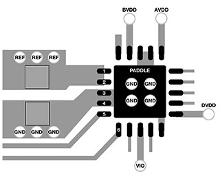
It is critical to place the reservoir capacitor close to the ADC’s reference input pin, using wide traces to connect it, as shown in Figure 10. The capacitor should have a low impedance path to ground using multiple vias to the ground plane. If the reference has a dedicated ground, the capacitor should be connected close to that pin using wide traces.
Because the capacitor acts as a charge reservoir, it needs to be large enough to limit droop and must have low ESR. Ceramic capacitors with X5R dielectric are a good choice. Typical values are in the 10 µF to 47 µF range, but smaller values can sometimes be tolerated depending on the current requirements of the ADC.
Insufficient drive strength is another issue, especially if low-power references or micropower reference buffers are used, as these typically have much higher output impedances that increase dramatically with frequency. This is particularly true when using higher throughput ADCs, as the current requirement is higher than at lower throughputs.
Excessive noise from either the reference or reference buffer, relative to the LSB size of the converter, can also result in stuck codes, so the voltage noise of the reference circuit must remain a small fraction of the LSB voltage.
For more information contact Andrew Athanasiou, Arrow Altech Distribution, +27 (0)21 555 1884, [email protected], www.arrow.altech.co.za
| Tel: | +27 11 923 9600 |
| Email: | [email protected] |
| www: | www.altronarrow.com |
| Articles: | More information and articles about Altron Arrow |


© Technews Publishing (Pty) Ltd | All Rights Reserved
 printer friendly version