


DC analysis of a power delivery network (PDN), commonly referred to as IR drop, DC power integrity or PI-DC, answers some fundamental questions that every digital (or analog) designer should ask and answer:
• Is sufficient metal provided between the voltage sources and loads to deliver adequate voltage to every load? Sufficient power and ground shapes? Sufficient vias, and are they large enough?
• Can I cleverly optimise the PDN shapes?
• What part of the design is most likely to heat (burn) up?
• Have I done something weird with the ground shapes?
Many digital designers are aware of the need for accurate signal integrity analysis, or how essential it is to understand the AC aspects of the PDN (for instance, how many decoupling capacitors are needed), but give little regard to DC PDN (PI-DC) analysis. PI-DC analysis is also critical, however, because it can provide critical insight into a design’s quality and save valuable design real estate and layers, ensuring a cost-effective digital design. The fundamental question it answers is fairly straightforward: Is there enough metal (in the case of a PCB, almost exclusively copper) between the power source and all the loads to deliver adequate power to those loads? For today’s small, integrated designs, answering that question accurately can mean the difference between success and failure.
Not long ago, digital design was dominated by large form factors – desktop PCs and large servers, for instance. In those designs, entire metal layers could be dedicated to power delivery, ensuring minimal voltage drop between the source and loads. Conservative rules of thumb could be used to estimate how much metal was needed, with little consequence if excess area was dedicated to power delivery. A digital designer only ensured the DC power delivery was ‘adequate,’ with little thought given to optimising power delivery shapes to minimise their area and layers.
Those days are gone. Even server designs are incredibly dense and board real estate too valuable to waste with overly conservative design practices. All metal dedicated to power delivery must be ‘necessary’; we don’t have the luxury to add unneeded layers or board size. PI-DC analysis provides a sophisticated means of ensuring the power delivery metal is not only adequate, but necessary.
PI-DC tool data
Voltage drop
A PI-DC tool provides data on voltage drop from the source to the loads due to resistivity of the power net. It can no longer be assumed to be zero due to an infinitely large power plane. As designs shrink, the concept of power planes may not apply. While a layer may be primarily dedicated to power delivery, that layer will probably be broken into many sections (nets) delivering unique voltages around the design.
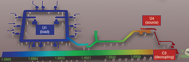
PI-DC shows how much voltage drop is induced in each net, allowing proper allocation of area to each voltage net. Figure 1 shows a typical 3D voltage plot of a 1,8 V power shape from its source (U4, a VRM) to the load (U1, an FPGA) along its two-layer path (vias are hidden in this view). Careful scrutiny of the voltage plot would show:
• Only 10 mV of drop between U4 (1,7 V, was de-rated by 5% from the nominal 1,8 V) and U1 (1,69 V).
• The single track from U4 to the FPGA voltage ring is the largest source of voltage drop.
• There is voltage drop from some of the vias – the colour of the net at the top of some vias is different to that of the bottom.
• There is no DC voltage drop between the source and decoupling capacitor, C3, as expected. Capacitors are treated as ‘open’ for DC analysis.
Current density
A PI-DC tool will also report the current densities (J) within the shapes of interest, allowing a designer to focus on making corrections to those areas with the highest current density (‘pinch points’ w/Jmax), if necessary. Notice this plot confirms what we concluded from the voltage plot, perhaps showing it in a more straightforward manner for some considerations.
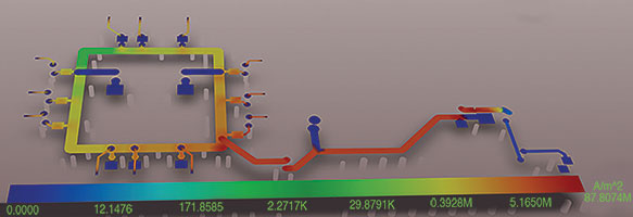
Unfortunately, there is usually no single threshold value to set as a limit for current density, so only relative values are often used. Thermal performance will depend not only on current density, but thermal dissipation of the system and even the cross-section of the shape.
Power deliver shape size
Without a PI-DC tool, the designer will probably use conservative rules dictating a particular width, based on the current the power delivery shape is carrying. There are at least two problems with that approach:
• Using the same minimum width independent of distance between the source and load(s) doesn’t often make sense; the same gauge wire isn’t used for 6’ and 100’ extension cords, for instance.
• Using that same width along the entire length of the shape not only wastes board real estate, it doesn’t represent the most efficient design of the power delivery shape.
A PI-DC tool will allow properly sizing the power delivery shape based on length, narrow the power delivery shape for short distances where necessary, and compensate for those constrictions by widening the shape where board real estate is more available. A PI-DC tool is critical for finding the optimum shape of power delivery nets.
Ground shape issues
Also, ground shapes can no longer be assumed to be infinite; today’s designs usually force limits on how much area can be allocated to ground. Those restrictions on ground area can cause significant voltages on ‘ground’; it no longer can be assumed to be zero.
Additionally, the problem of voltage on ground is more complex than for power nets; the actual voltage on any point on the ground net will be a superposition of the voltages induced by the currents from the various power nets. For instance, a design may have both 1,8 V and 3,3 V being delivered to a device. While the voltages on the two power nets are theoretically independent, the device will see a voltage on its ground pins that is the addition of the voltages induced by the 1,8 V and 3,3 V currents. It’s essential to understand and model that relationship accurately.
The good news is that, for DC, the superposition is fairly straightforward, and mere addition (or subtraction, for supplies of opposite polarities) is adequate. But be aware the ground shape size at any point will have to accommodate currents from multiple sources, whereas the power shape sizes are more straightforward.
Reference voltage
A PI-DC tool should be capable of providing DC voltage for a device using the ground voltage at that device as the reference voltage. The voltage relative to an arbitrary ‘ground’ point (such as the voltage source) is often meaningless. The currents in the ground shape may induce significant voltage on the ground net, and this must be comprehended in the DC analysis of the PDN.
Power delivery vias
A PI-DC tool also gives valuable insight into how many vias are needed, and how large, for power delivery. While this seems a trivial exercise, power vias typically consume valuable real estate on all layers, blocking routing on layers above and below their assigned power layers, and using too many or excessively large vias is a luxury today’s designs can’t afford. An especially ironic result of being overly conservative in power delivery via allocation is that those vias may perforate another power or ground plane, causing more problems for the design than they solve.
Comprehending temperature effects
Most PI-DC tools won’t directly provide the thermal effects of the current – how much they heat up the metal. This can be critical given the I2R relationship between current and power; even a small resistance can dissipate large amounts of energy if the current is high, leading to local hot spots and associated failures of the dielectric materials or conductors. However, PI-DC tools do provide information on the current density of power and ground shapes, allowing designers to optimise for low current density and therefore lower power dissipation.
IPC-2152 (previously IPC-2221) provides guidance on avoiding issues by providing minimum trace widths for acceptable temperature rise. PCB designers often misuse this, entering very conservative temperature rise values (1°C, for instance) and then using the corresponding wide trace width as the minimum width for their entire PDN shape from source to all loads. Applying the specification that way forces more area to be allocated to power delivery than is necessary, consuming valuable design real estate or requiring more layers for the design. To create the most efficient power delivery design,
IPC-2152 should be well understood, not applied blindly.
Instead of using an arbitrarily low allowed temperature rise value when applying IPC-2152, the digital designer should use a value representing a temperature rise that the dielectric material and metal can accommodate without risking damage or failure. For instance, permitting a 45°C temperature rise instead of only 1°C allows the minimum trace width to be reduced to 0,02” (blue) from 0,3” (red) for a 2 A current on 1 oz. copper. A PI-DC tool can then be used to ensure voltage requirements of all the loads are met when that minimum width is used.
The thermal issue is very complicated, and a thermal simulation tool might provide only limited insight due to the complexity of the problem. An accurate answer requires accurate models for the myriad components contributing to system thermal performance such as PCB material, numbers of layers, copper density, heat generation and dissipation of various components, airflow around the design, ambient conditions, etc. A digital designer will generally have to be conservative, but should take some critical aspects into account when considering thermal effects:
• Not all designs are the same thermally. A design known to reside in a cool environment with low-power components should require less accommodation for thermal effects than one consuming a lot of power in a very hot enclosure, for instance.
• Not all areas in a design are the same thermally. Special care should be taken where heat dissipation is poorest: on outer layers and under or near very hot components, for instance. Areas far removed from hot components will typically be less subject to thermal effects since the power is more efficiently dissipated. On the other hand, feeding a power-hungry device with narrow tendrils through its breakout is a recipe for disaster.
• How much is the current density increased? Heating is a function of the power consumed by the shape, proportional to I2R. Special care should be taken of the current density plots, and copper should be added where current density is at maximum. As mentioned, it is probably not possible to set a maximum current density limit since thermal effects depend on so many other factors, but PI-DC allows the designer to highlight the most likely areas of problems and gauge the relative ‘badness’ of design areas.
• Is the shape on outer or inner layers? IPC-2152 data indicate inner layers (stripline) dissipate heat more readily than microstrip layers (although this may depend on the amount of airflow over the trace, which will increase convection cooling; there may be some microstrip traces that dissipate heat well).
• Thermal requirements will depend strongly on the material used. Flex designs, especially those that are actively flexible, will typically be less tolerant of high temperatures than rigid PCBs, for instance.
• Is there relatively cool copper nearby that will dissipate the heat better than the dielectric material(s)?
Any designs that push the envelope of thermal performance should be carefully validated, of course. Aiding in the validation is the effect that conductivity of metals decreases with temperature, providing an indirect measurement of overall thermal performance; if the power shape is hotter than expected, it should experience a higher voltage drop. Measuring the voltage drop of an active design provides insight into the thermal characteristics of that design.
Thermal validation should be performed when conservative guidelines can’t be followed. It is critical for thermal issues to be considered for most digital designs, but blindly applying IPC-2152 guidelines in the most conservative fashion can lead to an inefficient design. Using PI-DC can lead to a design that satisfies both electrical and thermal requirements in the most efficient manner.
Avoiding garbage in, garbage out
A PI-DC tool must provide accurate results to be useful. Tool accuracy is not only a function of the (sophisticated) 2- or 3-D modelling engine used, but of the assumptions fed into the simulation. It is imperative users be very familiar with the critical assumptions and parameters fed into the tool.
Conductivity
The first parameter to get right is the conductivity of the metal used in the design. This is more involved than most realise. Most power and signal integrity tools, for instance, assume printed circuit boards use copper for their metal, with a conductivity of 5,88e7 S/m. Industry data indicate, however, that the electrodeposited copper used in PCBs is significantly less conductive than pure copper, only 4,7e7 S/m at 25°C. If validation and simulation results differ, metal conductivity should be verified.
That conductivity must also be adjusted for the actual operating temperature of a design. The conductivity of copper, for instance, drops 0,4% for every degree centigrade. The metal of a copper design operating at 125°C is 40% less conductive than the 25°C value! That difference must be comprehended in the simulation. It doesn’t do any good to have a highly sophisticated simulation engine if it’s operating on flawed assumptions. (Note: for designs operating at extremely low or high temperatures, even the linearity of the temperature coefficient, 0,4%/°C, must be examined for the expected ranges.)
Via models
Another fundamental assumption easy to get wrong is the size of the vias. Many PCB design tools use only a single value to represent the size of a particular via, and exactly what that number represents is ambiguous. Vias are usually assumed to be solid columns, but that’s often not accurate; they might not be completely filled and thus may be hollow columns, with both inner and outer diameters (ID and OD, respectively).
The actual cross-sectional area of the via depends on both dimensions: A large, but very hollow, cylinder can have less cross-sectional area than a filled smaller cylinder. For vias typically used in power delivery, most assume that if only a single value is given for a via, that value represents the drill size (outer diameter). The via is assumed to be completely filled, or best represented by a solid column. That assumption may not be valid, giving a flawed result.
Understanding exactly how to properly model vias means knowing how the via dimensions are specified and what the actual implementation of those specifications will look like (how the via will appear when cross-sectioned). Many tools do not allow a user to provide both an inner and outer diameter, only solid vias. If that is the case, and the vias are known to be hollow in actual implementation, the via outer diameter must be adjusted to represent the proper cross-sectional area.
Fortunately, finding the proper diameter for a solid column that has the same cross-sectional area as a hollow column with an OD and ID is a trivial mathematical exercise; it’s merely the difference of the two, OD minus ID. The challenge is to scale the vias properly when doing the simulation without having unintended consequences in the physical design.
Copper thickness
PCB outer layers used for power delivery represent an especially troublesome item to model. The copper thickness on PCB outer layers is a function of plating thickness, and that can vary significantly across the board. Be sure to measure the thickness of outer layers if used for power delivery and simulation results don’t match lab measurements.
Modelling loads
Finally, properly representing the loads seems straightforward at first, but is not. A designer might assume that, for a passive load like a resistor or diode, the load is best modelled as a resistor, and active components such as FPGAs should be modelled as current sinks. When active components are modelled as current sinks, however, it might be tempting to use the maximum current (Imax) as the current draw. When performing PI-DC simulations to gauge the voltage drop of the PDN, this is hard to justify and may lead to overly pessimistic results.
Maximum current draw will probably only occur when maximum voltage (Vmax) is applied. We typically simulate at the lower limits of the voltage range, and the current draw should reflect that in order to get accurate simulation results. A more reasonable model for an active load during voltage drop simulations might instead be a resistor whose value is a function of the device’s nominal voltage and current, Vnom/Inom.
On the other hand, some designers might have maximum current density values they are trying to avoid for thermal considerations (instead of minimum voltage levels for electrical consideration). For maximum current density simulations using PI-DC (for thermal considerations), Vmax should probably be used for sources, Rmin for passive loads, and Imax for active loads. This will give a more accurate representation of possible maximum currents.
When using a PI-DC tool, it is critical to understand all the inherent assumptions that went into the simulation and to validate those assumptions are accurate, or else the results might be meaningless.
Validating results
It is critical that any design is properly validated to ensure the accuracy of the simulation and the parameters fed into it. Fortunately, that is fairly straightforward for PI-DC. The voltage at each load can usually easily be measured, including using a local ground for reference.
Perhaps the most challenging aspects are to 1) find a means of ensuring all loads are consuming their maximum power when measurements are taken if the voltage on the ground shape might be a significant factor, and 2) properly comprehend the thermal effects on resistivity. Superposition might be necessary if exercising all loads simultaneously at their limits is not practical. In this case, the challenge will be to measure the voltage on ground at each load, relative to the same reference used in simulations.
For the thermal aspect, it will be necessary to have an idea of the actual temperature of the power shapes in order to calculate the correct metal conductivity, which varies as a function of temperature. This requires instrumentation not ordinarily found in most validation labs, such as thermocouples and IR temperature sensors.
If the measured voltages don’t match simulations, each of the simulation assumptions and results must be verified. We have tried to provide enough information into how to ensure proper assumptions, but how to check the results? The most fundamental data a PI-DC tool must get right is the resistance between the source and loads, and that usually isn’t directly provided. It’s fairly easy to construct a test circuit that will provide a value you can compare to an actual ohm-meter measurement of a bare design, however.
If the source is modelled as a 0 V battery and a load is modelled as a 1 A current sink, the voltage at the load directly represents the resistance between the source and load (ignore the sign of the voltage). For instance, Figure 3 demonstrates how to determine the resistance between a source (U4 pin 2 for power, J1 pins 2 and 3 for ground) and a load (U1, many pins) using a PI-DC simulator.
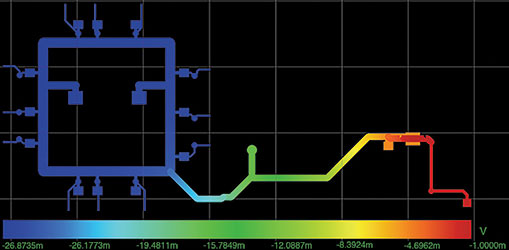
The results indicate there is 30 m of resistance in the PDN for U1 (note the -30 mV at U1 in Figure 3. To confirm this in the lab, place a 0 ohm ‘short’ between U4 pin 2 and J1 pins 2 and 3 (a large piece of metal, for instance), and measure the resistance between the power and ground pins of U1. A reading other than 30 m indicates an error in the simulation. Special techniques such as four-terminal sensing might be needed to measure these low resistances.
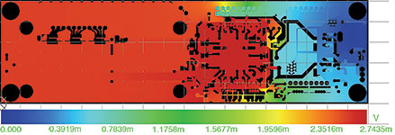
If it’s necessary to distinguish between the resistance of the power and ground planes, that can be done by analysing the voltage on each in this test circuit. Notice in Figure 4 that there are 27 m on the power shape (dark blue represents 27 mV, = 27 m) and that in Figure 5 there are 3 m on the ground shape (represented in red).
One critical factor to take into consideration during validation is the difference in resistivity due to temperature. The resistivity of copper, for instance, typically increases by ~0,4% per degree centigrade. The resistance of a PDN can increase 20% for a design running at 75°C, compared to room temperature of 25°C. This can also be an advantage. If the voltage of a system meets expectations when running hot under full load, the designer has assurance the copper isn’t much hotter than expected, reducing the possibility of catastrophic failures due to unexpected temperatures in that shape.
To be continued. The remainder of this article, which covers the topics ‘Other PI-DC results’, ‘Why do designs with errors work?’ and ‘Limiting current’, will be published in the next edition of Dataweek.
| Tel: | +27 12 665 0375 |
| Email: | [email protected] |
| www: | www.edatech.co.za |
| Articles: | More information and articles about EDA Technologies |


© Technews Publishing (Pty) Ltd | All Rights Reserved
 printer friendly version