


With the move into the digital age, outdoor signs and video walls are becoming more and more common. Nowadays, these electronic signs can be seen in stadiums, as street billboarding or advertising on buildings in cities, bus stops, gas stations, etc. As many of these applications have contact with the outdoor environment, protection of the electrical components, including the LED leads, is a must. Owing to technological advancement and also by the transition from radial to surface-mount technology (SMT) LED technology, there are a few challenges in video wall and signage applications. One of the main topics, the protection materials and methods of SMT LEDs for outdoor video walls, is discussed here.
Concretely, those methods are being addressed due to decreasing LED height, decreasing pixel pitch, coating material choice and the coating method. However, these challenges can be handled as shown by some realistic potting trials combined with environmental tests made by OSRAM Opto Semiconductors.
Basic construction of LED video walls
Most commonly, larger outdoor video walls or signs are made up of multiple modules with LEDs on them, which then define the finished product. As an analogy, one can think of the individual tiles on a bathroom wall as being video wall modules and the assembly of them next to one another as being the complete video wall (Figure 2).
These basic modules, also called tiles, can vary in size but often they are about 20–30 cm in length and width. Following a basic construction, they are composed of a frame, louvers, PCB(s) with LEDs and electronics. At the moment, louvers are a necessary part of the video wall tile as they act as sun blockers to increase the overall contrast, especially in outdoor application.
Advantage of SMT LEDs for video walls and signs
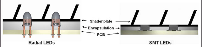
Until recently, the outdoor video wall and signage market has been dominated by an older lamp style: so-called radial LED technology. These types of LEDs are best described as having a bigger light emission dome and long metal leads. On the other hand, SMT LEDs tend to be smaller and do not have long leads.
There are numerous advantages in using SMT LEDs as compared to radial. One of the first advantages is the technology. Most of the innovation and progress in the LED business is happening on the SMT level. SMT LEDs have the advantage of greater package shape versatility, and are also available in multichip packages. The leads of radial LEDs can be as long as 30 mm. SMT LED packages could be less than 1 mm in height while the radial LED lamp can be as high as 10 mm and have a diameter of around 3–5 mm. Consequently, the size of the LED limits the minimum pitch values for video wall applications.
A further factor is the weight of the LED itself, which can make a big difference, especially in portable video wall applications such as concert and event setups.
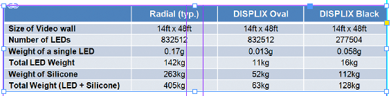
A single SMT LED like the Displix Oval from OSRAM Opto Semiconductors weighs just 13 mg, which is around 10 times less in weight than a typical lamp style LED (Figure 4). Due to the aforementioned differences in the LED height, the amount of protection material needed is consequently different.
Taking a simple estimation of a realistic video wall tile of the dimensions 24 x 24 cm and 16 x 16 pixels (pixel pitch 15 mm), the weights of different LED types and required protection material is compared.
For a better contrast, three LED types – 3,5 mm radial, Displix Oval, Displix Blackprint – were selected, with a setup of 3 LEDs per pixel for the radial type and Displix Oval, and 1 LED per pixel for Displix Blackprint (multichip RGB LED). As for the potting material, SE-9187L from Dow Corning, a one-component black silicone, was chosen.
Based on the setup and LED dimensions, a typical encapsulation height of 0,9 mm can be assumed for the Displix Oval, 1,9 mm for the Displix Black and 5 mm for the radial LED. Concretely, this would mean that there is a possible weight reduction of the lighting component of up to 6-7 times to use the Displix Oval and up to 3-4 times to use the Displix Black than a typical radial style LED (based on the raw weight data sheet values).
Extrapolating the estimation for one tile to a standard billboard size of 4,3 x 14,6 m, which has about 1084 of the above defined tiles, shows a significant impact on the system weight (Figure 5).
The challenge of LED outdoor use
Outdoor applications are among the most demanding areas for LEDs and LED light sources, because they are subject to or affected by many, sometimes conflicting, conditions. For instance, they may be affected by temperature, radiation, moisture, rain, dust, chemicals, gases and other natural phenomena.
To make a general outdoor qualification profile even more difficult, the geographical position and location have a tremendous influence on the type and magnitude of environmental occurrences, as well as the specific combination and interaction of varying ambient conditions. For example, an LED display installed in a Nordic rural town could be exposed to quite different conditions than a similar display at a busy city-centre traffic intersection or a town in the tropics.
However, as it has been seen for the video wall manufacturer, one of the most critical impacts on LED displays combined with outdoor use is the potential corrosion of the electrical components like PCB circuits, LED leads/pins, solder pads, contacts, vias, etc.
This corrosion could result in open contacts or shorts, and affect the functionality even to the point of a total breakdown of the display.
Therefore, the main quality focus in outdoor applications is the prevention of any kind of corrosion of the potentially exposed electrical metal parts.
Examples of protection methods
There are several popular methods that are used for environmental protection of signs and video walls.
Vapour deposition process in a chamber is usually how parylene is thinly coated (in the range of 20-30 µm) over the whole surface. Due to the fact that the parylene is applied in a gas state, even the smallest areas of the LED panel are uniformly coated, including the LEDs and all electronics. It is a very common method in certain military and aviation applications, for example. For such applications this could be a preferred method, but carries a potentially high cost and the parylene material often provides limited UV stability.
Another method is casting or LED encapsulation, meaning that the whole LED (including the light output area), is completely covered by dispensing a thick layer of a clear material (silicone, polyurethane, acrylic, etc.) up to a few centimetres.
There are applications – mostly in the general lighting field – where this method is desirable due to mechanical stability requirements, low process costs and a broad range of very cheap protection materials. However, the influence on the radiation characteristic due to a thick layer over the light output area does not make it very desirable for video wall/signage applications.
Similar to casting, conformal coating is a further method defined by some as the process of dispensing a thin layer of material of up to 300 µm over the whole LED panel (including the lens). With an advanced process called selective conformal coating, the material is dispensed selectively, specifically avoiding the LED light output area or the top of the LED package. It is one of the common methods in the signage industry, but it could take extra equipment, longer processing time and could require lower machine tolerances.
Finally, potting is a method commonly defined as the process of dispensing a thicker layer (typically greater than 300 µm) around the LED package, to cover the PCB surface and LED leads. This is one of the preferred methods of signage and video wall manufacturers, because the LED lens is not covered, the material potting height has more tolerance as long as it is below the package height, and the processing method is quite straightforward.
In the following sections, a proof of concept is shown using a potting process on the low-height Displix Oval providing easy adaptation to future LED technology.
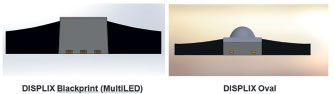
Figure 6 shows the way silicone is shaped due to the lower surface energy of the silicone as compared to surrounding materials it is in contact with. The material should not be placed on the top of the LED package or the lens as it could significantly change the LED radiation characteristic and/or the luminance, even if the material is clear.
Potting
Numerous potting materials could be dispensed to protect the LED metal contacts from the environment, such as polyurethane, acrylic, silicone, etc. As mentioned, the ever decreasing dimensions of LED packages allow smaller pitches and require different potting solutions.
A lot of video wall manufacturers have chosen RTV (room temperature vulcanisation) silicone (polydimethylsiloxane – PDMS) as a preferred material due to the advantages of this material. The silicones made for these applications possess the following characteristics:
• Suitable for use over a wide range of temperatures.
• Provides stress relief and protection of delicate component leads.
• Good moisture and humidity resistance.
• Good adhesion to no-clean, low solids and lead-free flux technologies.
• Processing versatility.
• Easy reparability.
• Low toxicity.
Due to the high density of components on the PCB tile, a highly flowable and self-levelling silicone material is necessary.
Experimental potting setup
Materials
For the experimental potting trials, three different LED types – Displix Oval, Displix Blackprint and the Displix Black – were used (Figure 7).
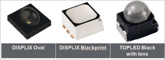
These LEDs are especially designed for video wall and signage applications. The Displix Oval has a footprint of 2,7 x 2,1 mm and LED foot height of 0,9 mm with an oval lens on top, whereas the multi-LED Displix Black and Blackprint have 4,5 x 4,5 x 1,9 mm package dimensions.
Of the many products available on the market, the one-component black RTV silicone SE-9187L from Dow Corning has been selected, based on its low viscosity for enhanced flow and self-levelling to achieve an homogenous and flat coating. Furthermore, the very low surface energy of silicone will allow the material to efficiently wet out the substrate into the tiniest corners of the components, creating good coverage.
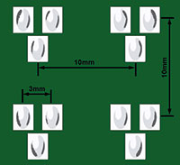
Two types of PCBs were used. The first was a PCB with standard LED alignment which is commonly used by OSRAM Opto Semiconductors for LED testing and qualification. The second type provided the specific small LED pitch with the small Displix Oval LED and with a small pitch of 10 mm, and LED to LED intra pitch distance of ~3 mm (Figure 8).
Equipment
The selection of the best possible equipment is based on the type of material (mainly one-component or two-component), the size of the products/title, the required accuracy and repeatability of the application and the required cycle time per product. Secondly, the required investment should also not be forgotten – investment in the initial equipment, as well as daily maintenance costs.
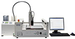
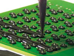
Here, the Nordson DIMA Dispense Master DD-500 in combination with the Nordson DIMA DD-5131 dispense valve were selected since small quantities but high varieties of different shapes have to be performed. The machine (Figure 9) was a good candidate for the test because it is flexible, the boards can be placed manually and it is an easy to operate desktop system.
This desktop robot is a XYZ-system that is capable of handling boards up to 400 x 600 mm with a dispensing work area of 320 x 420 mm and a Z-stroke of 87 mm. The total size of the system is 700 x 700 x 550 mm (L x B x H). The maximum speed of the system is 80 mm/sec and the accuracy is at 150 microns.
The Nordson DIMA DD-5131 dispense valve (suitable for 1K or 2K compounds) can be mounted to the gantry with a head that can move in the XYZ-direction. The camera is a standard feature in this machine that makes programming more user-friendly, but it is not necessary for the process. During the tests the camera helped to program the dispense positions.
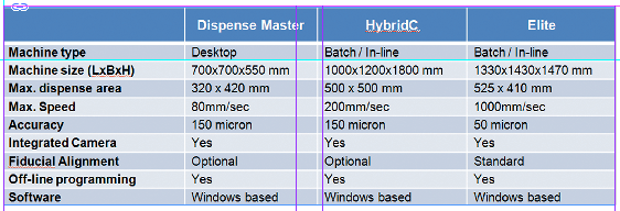
Other systems available on the market provide in-line capabilities, higher speed, better accuracy and a larger work envelope. The better machines for in-line capabilities, such as the Dispenser Elite line from Nordson DIMA, provides higher speeds (10x faster dispensing as compared to the Dispense Master line), larger sample area and other technical features such as extremely good accuracy that provide fast in-line performance (Figure 10).
Dispensing procedure
Potting can be done by applying material in one position, using the material flow to slowly fill up a complete area. However, in the case of LED boards, the accuracy needed to fill up the boards nicely to the edge of the LEDs needs a more precise movement of the dispense nozzle during the potting sequence.
The main challenge in process optimisation is to not cover the top face of LEDs. In general, five parameters mainly determine the dispensing process, and influence the dispensed line widths. These are:
• The pressure with which the material is being supplied from the original packaging (syringe, cartridge, pail), creating a certain material flow.
• The speed of dispensing (motion of head).
• The diameter and style of the dispense needle.
• The stroke of the dispense valve.
• The distance of the dispense needle from the LED board.
For an optimised process and potting result, the machine parameters have to be adapted to the material used and its properties. If cycle times are very critical, parallel processing is
another way to speed up the process. This can be done by duplicating the amount of nozzles in the dispensing system and upgrading to faster in-line systems.
For process control/monitoring and to achieve board-to-board repeatability, there are several more options available. One option is to control all pressures within the machine that are being used to apply the material onto each board. Secondly, one can make sure that the material reservoirs being used cannot run empty without providing a warning signal.
To make sure that every board will contain the same amount of material, flow monitoring can be used. Through flow monitoring the amount of material flow is monitored during the dispense cycle, making sure that the exact same amount of material is being applied on every single board.
The chosen RTV silicone can be repaired, though silicones generally do not adhere well to themselves. Therefore it is recommended to consider the optional use of a primer or gently roughening the surface to improve adhesion. When touching up the solder joints of a rework site with new coating, it is imperative that the coating surfaces are clean.
Curing procedure
The silicone potting material Dow Corning SE-9187L readily wets the substrate, providing a suitable interface for adhesion to develop. However, the PDMS molecule itself will not bond chemically to a surface. To achieve a molecular bond between the silicone and a substrate, an adhesion promoter is added to the product formulation.
The cure of RTV silicones is initiated by moisture from the air that permeates into the silicone and reacts with the titanate catalyst. The resulting intermediate then reacts with the cross-linker and with the polymer. Finally, all of the remaining species complete the cross-linking reaction to form a uniform coating/potting layer. Because the first step depends on contact with moisture from the air, the outer layer of the coating will begin to solidify first. A ‘skin’ of cured coating will form as the cure progresses from the outside inward.
At this point, the coating/potting layer can usually be handled and subsequent manufacturing steps can proceed. As the cure reactions proceed through the depth of the coating, the materials will completely solidify. Full cure occurs when the material is fully hardened and strong cohesive adhesion has been obtained to the PCB.
Note that adhesion typically lags behind the cure and may take up to 72 hours to build up, depending on the applied coating thickness and curing conditions. Low heat up to 60°C can improve the cure speed, but should be applied with caution taking into consideration the tack-free time before heat exposure (typically 10 minutes). If the ‘skin’ is formed too quickly, solvents can be trapped under it, causing the creation of bubbles.
While moisture from the air is mandatory for cure to progress, only a very small amount is actually needed. Even though a high humidity level accelerates the cure in a very deep coating thickness, excess moisture will slow down the cure in thin sections. This occurs when the catalyst near the coating surface becomes saturated with moisture and becomes deactivated. This can significantly slow both the skin-over time and the time to full cure.
On the other hand, moisture levels below about 5% relative humidity will slow down the cure significantly. Recommended relative humidity values range from 30% to 80%. Elevated temperatures greatly lessen the effects of humidity on the cure speed and no additional humidity is necessary in the oven (most of the ovens running at 60°C will have a relative humidity close to 10%).
Note that a good ventilation flow over the PCB is important to efficiently remove the solvents, but caution should be taken as too large air flows can cause wrinkles in the surface.
Potting results
The main purpose of the potting tests was to verify and test the suitability of the potting material concerning its use in LED video wall applications, especially with low-height SMT LEDs with a tight pitch. For the potting with the one-component RTV silicone from Dow Corning (SE-9187L), a 20-gauge plastic tapered needle (inner diameter of 0,6 mm) was used. The speed of dispensing was limited to 55 mm/sec and the pressure used on the material (supplied in 175 ml cartridges) was set at about 2 bar.
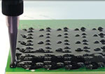
The distance between the dispense needle and the LED board was set to 0,7 mm, creating a nice flow of material providing a 6 mm line. The material was dispensed in a simple way with vertical and horizontal lines, not especially adjusted to the LED alignment (Figure 11).
One of the most critical areas seemed to be small sections that needed to be covered between LEDs within a pixel, in this case small lines of 0,9 mm width. But as the trials have shown, the selected silicone flowed well between the LEDs, even filling the empty spaces within single pixels.
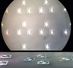
This could be partially attributed due to the capillary effect and the optimised dispensing process. Even though when looking at the board from further away, it almost seemed that the LED package and the lens were covered by the silicone material (Figure 12), after close inspection with a microscope it was confirmed that the package and the lens were not covered (Figure 13).
Near the PCB edges the material forms a decreasing coating layer and stops at the rim of the board without overflow depending on the deposited quantity, but a frame for potting was not needed. In one trial, an elevated temperature cure was done according to the material data sheet of the RTV silicone (Dow Corning SE-9187L) and it was discovered that the strong air flow caused wrinkles in the ‘skin’ formation of the silicone during the cure. This should be avoided by using a suitable oven as mentioned in the curing procedure section above.
The potted test boards were cured at room temperature for 24 hours and then were transported. According to the data sheet, greater than 90% of full physical properties should be attained within 24 to 72 hours, therefore possibly allowing careful handling which in return could save time in the manufacturing process. Furthermore, the potting process was done on different days with varying humidity levels in the room (it is an advantage of this material that it does not need high humidity levels to complete the curing process). Handling was easy and the material showed good repeatability in multiple trials.
The tested silicone has an adhesion promoter inside, and from the first look showed good adhesion to the PCB after the full cure. In a standard lap-shear test the adhesion strength to a typical FR4 board was measured to be 0,2 MPa, with 100% cohesive failure.
The potting process for the Displix Blackprint was similar as with the Displix Oval, except that the LED to LED wall space was larger (5,5 mm with a 10 mm pitch) due to the 3-in-1 chip package, having even less accuracy requirements in the processing.
The remainder of this article, which details a regime of environmental tests conducted for this particular application, can be accessed online at www.dataweek.co.za/+k3533
For more information contact Petrus Booyens, OSRAM Opto Semiconductors, +27 (0)79 525 1779, [email protected]


© Technews Publishing (Pty) Ltd | All Rights Reserved
 printer friendly version