


Today's system designs are growing in complexity, requiring larger amounts of memory for high-performance buffers and other local data storage. System designs that require both logic gates and memory are sometimes implemented in a single FPGA device containing embedded SRAM. The embedded SRAM in these FPGAs can be implemented as synchronous or asynchronous memory functions such as register files and FIFOs. FPGAs with on-chip RAM provide an easy solution for both logic and memory needs. However, selecting FPGAs containing blocks of SRAM to meet system memory requirements may increase the overall cost of the system.
Actel's SX-A/SX FPGAs were designed without on-chip SRAM to maximise their price/performance advantage. Small blocks of distributed memory can be implemented with registers using Actel's ACTgen macro generator. Larger memory requirements can be met with external RAMs that efficiently interface with the Actel devices. For many applications, an FPGA with an external memory device can meet functionality requirements more cost effectively.
Actel has a paper that details the price/performance advantage when implementing both simple and complex SRAM memory functions in the Actel SX/SX-A devices. This is a shortened overview; the full copy is available from ASIC Design Services, local distributor for Actel in South Africa.
Memory types
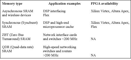
There are many types of external SRAM memory devices, each providing features tailored for specific design requirements. Table 1 describes some of the most common SRAM types, applications for which they are best suited, and FPGAs that contain this type of SRAM.
When a system requires a single large block of memory, an external SRAM component can provide any variation of density, speed, price, type, package, etc., while also allowing for easy future upgrading to larger-density or higher-speed devices. Separate components enable the designer to select the SRAM storage requirements independently of FPGA gate count - flexibility not available in an FPGA with SRAM blocks.
Size
For applications with simple memory requirements such as small FIFOs, external memory is not required with the SX/SX-A devices. With such devices, it is reasonable to use up to 25% of the sequential cells as memory equivalents. For example, one might use up to 1000 registers in the A54SX72A device to implement local distributed memory while leaving about 3000 registers available to implement logic functions. For larger, more complex memory requirements, an external memory device that is specifically suited to the application can be used.
Some key advantages of using an independent external memory device rather than the embedded memory of an FPGA are:
* The RAM density and FPGA gate count can more closely match system requirements. Choosing an FPGA with embedded RAM can waste gates in order to obtain the required RAM size. This results in increased die area and system cost.
* The external RAM solution offers a simple migration path to higher-density RAM or FPGAs for future system upgrades. All that is needed is a simple component change plus minor changes to the interface logic. By using a standard JEDEC package that supports multiple densities (eg Micron and IDT have pin-compatible 2, 4, and 8 Mb RAM devices) the original circuit can be designed to accommodate various memory sizes.
Performance
Using FPGAs to interface with high-speed memory devices often enables meeting demanding clock-to-output or input setup-and-hold specifications. When writing to memory, the FPGA must output the data and control signals within a single system clock cycle as well as meet the external device's input setup-and-hold requirements. When reading from memory, the data access time (the time for the addressed data to appear on the bus) and the input setup-and-hold times on the FPGA are critical to performance.
Actel's SX/SX-A FPGA families are optimised for this application because the I/O cells are designed to offer the lowest clock-to-output delays in the programmable logic industry. The SX/SX-A families achieve worst-case clock-to-output delays of less than 4 ns and require 0 ns hold time and 0,5 ns setup time. This supports synchronous system performance of over 200 MHz when interfacing with external memory components. The global clock networks are also optimised for ultra-high performance and, in conjunction with their fine-grained antifuse architecture, are able to support internal clock rates in excess of 300 MHz. SRAM-based FPGAs usually have larger die sizes than antifuse devices because SRAM switches must reside next to the gates. On the other hand, antifuse switching elements can be the same width as routing channels and located above them; therefore, the antifuse switches do not add to the die size. Also, the larger die sizes of the SRAM-based FPGAs cause additional delays in the device due to the increased length of the routing tracks.
Price comparison
The paper uses three design examples to demonstrate the cost effectiveness of the Actel SX-A family when combined with external SRAM components. The Actel SX-A FPGA family with external SRAM is compared with the Xilinx Virtex, Altera FlexE, and Altera Apex FPGA families with internal SRAM. Actel bases all its prices on 1-99 piece quantities of standard-speed-grade FPGAs.
The three examples compare alternative implementations of an FPGA with either: 256K, 1 Mb and 4 Mb SRAM and give a normalised comparison of the total system cost.
Actel also shows that, in addition to having the advantage of lower system cost, the Actel solution can actually offer a lower component count. Volatile SRAM-based FPGAs require a second memory device for configuration at system power-up, resulting in a two-chip solution. If an external SRAM is also needed, this requires a third chip. Actel's nonvolatile FPGAs do not require a boot PROM at power-up, thus lowering the overall system component count.
Other considerations
The paper continues with a look at implementing distributed memory and interfacing to external FIFOs. It gives a VHDL design example to demonstrate the SX-A's high-speed interfacing capability. A ZBT interface for use in very high-performance networking systems is described. In order to interface to a high speed ZBT SRAM device, an FPGA must have very fast input/output (I/O) buffers. Every cycle can either be a read or a write cycle, and the most challenging timing specs are those involving bus turnaround - from a write to a read cycle or a read to a write cycle.
Conclusions
The SX-A and SX FPGAs from Actel are very high-performance programmable logic devices. When storage space is needed, they can implement small quantities of storage on the chip using logic functions. When large quantities of storage are needed, an external memory device is recommended. The larger the memory requirement, the less attractive SRAM FPGAs become, especially when additional support devices like boot-up PROMs are considered. The flexibility of selecting optimally-sized memory devices from multiple vendors, combined with cost savings arising from choosing an FPGA with optimal gate count, makes a compelling case for implementing a two-chip, FPGA plus external RAM solution.
For further information or a copy of the full paper, contact Kobus van Rooyen, ASIC Design Services, (011) 315 8316, [email protected]
| Tel: | +27 11 315 8316 |
| Email: | [email protected] |
| www: | www.asic.co.za |
| Articles: | More information and articles about ASIC Design Services |


© Technews Publishing (Pty) Ltd | All Rights Reserved
 printer friendly version