


Advanced packages (eg PBGA, CBGA, CSP and new MLF, LLP, LGA) require a new rework process. The latest types of components launched by the leading component manufacturers have increased the need for process control in rework. These packages are referred to by the generic name Land Grid Array (LGA) or the specific package names - Leadless Lead-frame Package (LLP) and Micro Lead Frame (MLF). These packages are unique because they contain multiple pad sizes and shapes on the same device. They are also soldered with all terminations on the underside of the package, similar to BGAs.
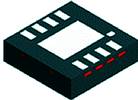
These components lend themselves to normal assembly techniques such as screen-printing the PCB, automatic pick-and-place, then convection reflow. The LLP design has a large centre pad that is often soldered to the PCB as a ground or power connection. They can also act as a heat spreader to the PCB substrate. This helps keep it cool and controls expansion of the part to the substrate so that the TCE (thermal coefficients of expansion) tolerances of the part to the PCB material are minimised.
The rework process for LLPs requires all the pads to be soldered to the same height or the potential for small land connections could be an issue. The solder paste volume used for the centre and array pads needs to be controlled to achieve good, reliable joints.
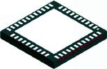
New style packages: LLP leadless lead frame package
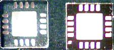
Since LGA components are more densely packed on the PCB, they need different processes to be successfully reworked. Because the pad sizes on the component differ, the solder volumes are difficult to control by using only a soldering iron to tin the lands. This is especially true of the sample components illustrated below.
Because the packages all have different pad sizes on the same device, a new rework method has been developed. Using the old rework process, where the pads of the PCB are 'tinned' with a solder iron, the correct solder level required to get consistent, equal solder joints was not achieved. Here, larger pads are tinned to a higher height, causing the smaller pads to be lower in height. This is evident in an X-ray after reflow, where different solder volumes on the pads are seen.
Only the rework process is changed
Printing on a PCB, when fully populated, is difficult because of the size and packaging density around the devices. Today, small chip components are often very close to the packages. To alleviate this problem, a method of printing on the package has been developed. Here, the standard thickness of paste used in assembly is printed on the package. If this method is followed this will control the solder volume for replacement in the rework process.
The rework process is as follows:
* Remove package from the PCB with a convection rework system, such as Metcal's APR-5000 array package rework system, or a comparable machine. Clean solder pad array on PCB to remove old unlevelled solder using a small blade tip and solder station. Place the solder wick under the blade tip to soak up the solder. Next, clean the PCB with a cleaner and lint-free wipe to remove flux residue left from solder wick.
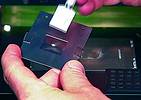
* Select a new part and use the component clamp to secure in stenciling template. Pin 1 location is marked on the plate and underside of the component with a small location pad that is not soldered or printed. Print the solder paste on the back of the template. The template comes with a spatula that matches the aperture size of the print window, so no pads are missed in printing. The spatula has a step etch and one tip is to print twice at 90° to ensure the print windows are completely filled.
* Solder paste 'education' in the rework area may also be needed. Many operators need to understand the importance of cleanliness in operation and not leaving paste tubs open. A paste pallet is a good solution. The pallet is a small stainless plate that is used as a mixing and paste preparation plate. Take a small amount of paste out of the tub and reseal the pot. Never use the back of a PCB as a plate, as the spatula will remove solder resist and fibre. Also, never use solder paste from syringes, as this dispenses paste at a different viscosity and will slump easily. Standard type-4 fine pitch paste works well on 20 mil pitch components. Once paste has been applied, place template on rework machine and pick package out of template with paste on underside of package.
* Inspect, on rework machine, with a vision system to look at the underside of the part. If all pads are printed correctly then alignment can be done and the component placed on the PCB. If not, the package will need to be cleaned and reprinted or a new part printed. One major advantage is that no paste is placed onto the PCB until the printed part is ready, eliminating the process of re-cleaning the PCB. When placing the part, it is important to control this part of the process, so that the part is gently placed onto the PCB. Too much force could make bridges form. Usually, the solder paste is 5 mils and can be just placed or lowered a few mils onto the PCB; however, do not push too hard.
* Now the reflow stage needs to be done, similar to a full conveyer reflow oven. Because solder paste is used, a good solder profile is needed to avoid defects such as voids or opens. If a multizone reflow profile is not performed, some voids may appear in the large centre pads. The best method is to duplicate the oven profile. If is not possible and live interactive software is available, then thermocouple the PCB next to the component and create a profile. Use multi-zone reflow. This involves multiple preheating of air, including top and bottom control, the same as a full convection reflow oven. i.e preheat, soaking, ramp, reflow, and cooling zones. This will solder these packages to the same standard as a production assembled part.
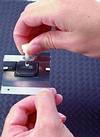
The example pictured shows a BGA stencilling template with a component in the template. This apparatus was originally made for LGA components and then applied to standard BGA and CSP parts. By printing on the part, the solder level can be increased to that which is used in production-assembly, thus increasing the quality of rework and reliability. This method is ideal for LLP and similar parts, with their different size pads, because they can be reworked easily and reliably.
Considerations
Placement must be done with a prism to overlay the component image to the PCB pads. Hand placement is not recommended due to the lack of accurate depth control needed to place the part without squashing the solder paste. Care must be taken to ensure reflow is the same as production soldering. If parts are reflowed for too long, grainy joints can occur and if reflow is too fast, a void can occur. Cooling is an important stage to get the PCB temperature down, to maintain control of the time above reflow.
For further information contact Metcal representative, Test & Rework Solutions, 011 708 3451.
| Tel: | +27 11 704 6677 |
| Email: | [email protected] |
| www: | www.testandrework.co.za |
| Articles: | More information and articles about Test & Rework Solutions |


© Technews Publishing (Pty) Ltd | All Rights Reserved
 printer friendly version