


Higher mask cost and increasing minimum lot sizes, two economic trends of the semiconductor industry, are making FPGAs increasingly more cost-effective compared to the competing ASIC solutions. As a result, the market share of FPGAs and along with it, the 'value' of designs implemented in FPGAs continues to grow. As FPGA design 'value' increases, so does the need for design security in FPGAs.
At the very least, designers would like to duplicate in FPGAs the level of design security they had with ASIC technologies. This article describes several distinct design security issues and concepts, the contrasts between the design security of competing FPGA technologies (SRAM, antifuse, and Flash) with the incumbent ASIC technology. A new business model enabled by the security capabilities of nonvolatile antifuse Flash-based FPGAs will also be discussed.
Design security concerns
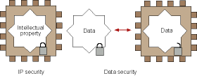
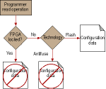
There are two distinct classes of design security needs (Figure 1):
* Intellectual property (IP) security: the designer wants to protect the design or IP in the FPGA or ASIC platform from being 'cloned' or reverse-engineered.
* Data security: the designer wants to prevent the data being sent to or from the FPGA or ASIC platform from being copied, corrupted or otherwise interfered with.
IP security is the primary concern of companies or IP developers whose competitive advantage is derived from their ability to implement the design. It is also the primary concern for manufacturers of mid- to high-volume consumer electronics whose market share and profitability is eroded by 'knock-off', 'cloned' or counterfeit versions of their product.
Data security is the primary concern in cryptographic or financial applications. Users of such applications include the military (nuclear weapon systems or communication systems), financial institutions (automated bank tellers), consumer electronics manufacturers (pay TV and set-top boxes) and corporations sensitive to copyright infringement (game manufacturers).
IP security depends upon three factors:
* The value of the design or secret being protected. This can range from nearly infinite (securing a trigger for a nuclear device) to very low (the stored value on a single phone card). Often the value has a time component (the market window for a consumer product or the usable life of a set-top box).
* The cost to implement security measures. These can vary from zero to very high (epoxy-encased circuit boards installed in locked chassis with round-the-clock surveillance or a cryptographic key infrastructure).
* The expected cost to attack or defeat security measures. These can vary from very low (cost of copying a boot device for an SRAM FPGA) to prohibitive (evading surveillance to remove and reverse-engineer an epoxy-encased circuit board).
The cost the designer will incur to protect his design will be proportional to the value he assigns to the design.
Defending a design from attack
The ability to reverse-engineer an IC can be rated at three different levels, corresponding to varying degrees of security:
* Level I: devices are insecure because they can be easily reverse-engineered by a somewhat knowledgeable individual with low-cost, easily-accessible tools. These people are usually interested in end-user products such as phone cards, debit cards and set-top boxes.
* Level II: devices are moderately secure because reverse-engineering can be done by a highly knowledgeable individual, often someone with inside knowledge and access to expensive lab equipment. (Individuals at this level are usually associated with a commercial enterprise such as a game copier.)
* Level III: devices are highly secure and reverse-engineering can only be done by a government-supported lab with 'unlimited' resources.
ASICs are secure to a Level II attack: On its own, ASIC technology (standard cells and, to a lesser degree, gate arrays) is thought to be Level II. This technology has been employed in all of the security scenarios previously mentioned. For against Level III attacks, additional measures such as epoxy-encasing and explosive devices must be employed. Methods of attacking ASIC technology involve expensive equipment and tools, including:
* Cleanly imaging and etching away successive layers of a device and post-processing the images to render clean polygon images of the circuitry.
* Building on the above techniques, Chipworks has developed software to automatically generate circuit schematics from the polygon images.
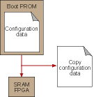
SRAM FPGAs are susceptible to a Level I attack: As mentioned, market forces are enabling FPGA technology to continually capture ASIC market share. However as the value of the designs implemented in FPGAs increases, security limitations of the dominant SRAM-based FPGA technology begins to limit market penetration potential. SRAM-based FPGA technology security limitations are well known, as the devices are easily cloned by copying a bitstream sourced to the SRAM FPGA by either a nonvolatile boot PRIM or a microprocessor (Figure 2), corresponding to a Level I attack.
Some SRAM FPGA manufacturers have incorporated a defence against this cloning attack. This defence is comprised of an on-chip bitstream decryption engine with an on-chip key that is loaded into battery-powered on-chip memory on the board by the board manufacturer (Figure 3).
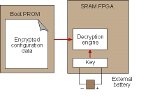
The bitstream loaded in the boot PROM can then be encrypted and therefore is not usable for cloning without knowledge of the on-chip key. While this defence is effective, it does come with significant costs to implement, including:
* Cost to implement and maintain an encryption key database or infrastructure at the board manufacturer.
* Reliability cost due to the battery-powered key storage mechanism. If the battery fails in the field, the board will fail.
Nonvolatile Flash and Antifuse FPGAs are more secure than ASICs: There are two nonvolatile FPGA technologies that are even more secure than competing ASIC technologies. They are antifuse-based FPGAs and Flash-based FPGAs. These two technologies derive their security from:
* Nonvolatility, which enables them to be configured before they are shipped to the end-user. Unlike SRAM technology, there is no bitstream that can be intercepted.
* Difficulty in determining the state (on or off) of the programming elements on a programmed part. In contrast with easily-visible vias on an ASIC, it is very difficult to determine whether a given programmable antifuse or Flash switch element is on or off.
* A large number of switch elements (millions on the largest devices). Given that the state of a single switch is difficult to determine, trying to determine the state of millions is prohibitive.
Direct physical attack of antifuse FPGAs
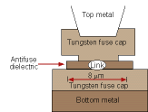
As previously stated, determining the state of an antifuse is exceedingly difficult. Antifuse-based FPGAs use a small piece of dielectric, usually smaller than 1 µm square, as an open switch between two metal lines. Where a connection between two metal lines is desired, a programming pulse is used to short out the dielectric. This short is less than 100 nm in diameter. These shorts are not visible when viewed from the top. Therefore, in order to physically identify them, it is necessary to de-process or cross-section the devices. Rather than being a precise method, this involves trial and error and typically requires that several cross-sections be done to find just a single link shorting out the dielectric (Figure 4).
Direct physical attack of Flash-based FPGAs
As with antifuse-based FPGAs, Flash-based FPGAs utilise switches to connect and disconnect intersecting metal lines. A single floating gate is charged or discharged to set the state of a switch that connects two metal lines. Since there is no physical change in the programming device or switch device, there is nothing to detect by any material analysis; there is only a change in the number of electrons on the floating gates. Because there is no observable change in the Flash-based switch when programmed, a Flash-based FPGA is more difficult to reverse engineer than even an antifuse FPGA.
Other methods
Several other advanced methods of attack have been developed - but with considerable expense and/or difficulty:
* IBM developed a very advanced technology that allows one to actually look at the logic states of the metal lines. This is accomplished by placing a crystal of lithium niobate over the feature whose voltage is to be monitored. The refractive index of this substance varies with the applied electric field, and the potential of the underlying metal can be read out using an ultraviolet laser beam. This technique allows a 5,0 V signal of up to 25 MHz to be read.
* Another technique (recently declassified) developed at Sandia Laboratories utilises an infrared laser to which the silicon is transparent. It is then possible to shine the laser from the backside to induce photocurrents that are affected by the logic state and thus determine the logic state of a specific transistor.
Finally, both antifuse and Flash-based devices are architecturally-designed to prevent attack on a programmed device with a programmer or other electronic means (Figure 5). Both contain circuitry to lock the device by disabling the programming and readback capabilities after configuration. Care has been taken in the design to make the locking circuitry difficult to defeat through either electronic or direct physical attack. In antifuse FPGAs, fuses programming is essentially a one-way function. Thus the architecture of the antifuse-based devices makes electronic readback impossible, even if the locking mechanism is not used.
Unique business models with secure nonvolatile FPGAs
The last decade has seen a dramatic shift in the semiconductor industry from a few horizontally integrated companies to dozens of fabless semiconductor companies using the services of silicon foundries. The next big shift expected was continued vertical fragmentation with hundreds of design services and IP companies providing their services to system level architects and integrators. That expectation has failed to materialise and the design services and IP providers are still struggling with how to capture their share of the value chain.
Secure nonvolatile FPGAs offer solutions to overcome two large barriers in this struggle. The first barrier is simply security. Just the concern that design company has in protecting their intellectual property sets in motion legal and administrative activities and costs that, in the end, prove too high to justify all but the largest engagements. The industry has spent a lot of effort developing design encryption schemes that protect the design at the netlist level, but it is still exposed to a trivial cloning attack if implemented in an SRAM FPGA. In contrast, a nonvolatile antifuse or Flash-based FPGA prevents such an attack and offers even more security than an ASIC implementation.
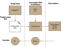
The second dampener on the industry is that the design services company has no easy and trustworthy way to charge a royalty for their services. All the money must be made in up-front licensing fees that, again, can only be justified in the largest engagements. With secure nonvolatile FPGA technologies, the design services company can become a virtual ASIC company and ship pre-programmed FPGAs with a nominal mark up or royalty charge above the cost of the unprogrammed PFGA. If the FPGA vendor is trusted with the programming files, end-customers can order pre-programmed units from the FPGA vendor who takes care of charging the end-customer for the mark-up and forwarding the mark-up amount to the design services provider (Figure 6). This flow eliminates operational costs for the design services company while allowing them to make a nominal amount for each unit rather than trying to charge for the entire engagement up front.
Conclusion
As the complexity, capabilities, and market share of FPGAs increases with respect to competing FPGA technologies, the need for securing the designs implemented in FPGAs increases. SRAM FPGAs are inadequate in this regard as they are exposed to a Level I cloning attack. On the other hand, nonvolatile antifuse or Flash FPGAs are even more secure against attack than the ASIC technologies they are replacing and therefore satisfy an increasingly important market requirement. Furthermore, the programmability and security provided by these technologies can be employed to solve a latent need in the semiconductor industry: The need for design services and IP suppliers to claim their share of the value chain by charging a royalty over the life of the design rather than having to get all the value in up-front licensing.
For further information contact Kobus van Rooyen, ASIC Design Services, 011 315 8316, [email protected]
| Tel: | +27 11 315 8316 |
| Email: | [email protected] |
| www: | www.asic.co.za |
| Articles: | More information and articles about ASIC Design Services |


© Technews Publishing (Pty) Ltd | All Rights Reserved
 printer friendly version