


Qvar is an electrostatic sensor from STMicroelectronics that can be used for human presence and motion detection, touch detection, and user interface (UI) applications.
All materials are comprised of atoms, each of which has a positive nucleus with electrons surrounding it. When two different materials are brought together in close physical contact such as rubbing, one of the materials may attract electrons more than the other, so some electrons are pulled from one material to the other. When the materials are separated, one of them has gained some more electrons (negatively charged) while the other has lost some (positively charged), depending on the working function of each material. Such a phenomenon is often known as the triboelectric effect, where the prefix ‘tribo’ means friction. Since the triboelectric phenomenon exists widely in our daily lives, electrostatic sensors can be used to detect or sense a diverse range of human activities, mechanical systems, or industrial processes.
Qvar stands for electric charge (Q) variation (var). It is an electrical potential sensing channel able to measure the quasi-electrostatic potential changes, enabling applications such as:
• Contact and no-contact human motion detection.
• Human motion gait analysis.
• Human presence detection.
• A user interface (UI).
• Water detection.
An electrostatic charge is expected on a material whenever it comes into contact with another material, or a solid or liquid surface. The level of charge is usually unpredictable, but it can be detected by means of an electrode and an electronic signal conditioning circuit. A signal is derived from the electronic circuit due to the fluctuations in the electric field resulting from the passage of the charged particles.
When a sensor works by electrostatic induction, the sensing principle may be explained in terms of an equivalent capacitive sensor. This is because the charged object can be modelled as a plate of a capacitor while the electrode itself is modelled as the other plate. The movement of the charged object, with reference to the electrode, changes the distance between the two plates and hence the value of the capacitance. Similarly, the quantity of charge on the object, and hence the voltage across the plates, may change with time.
It is well known that electrode features such as size, shape and material are important factors that may produce different Qvar channel results. For instance, there exists a linear relationship between sensitivity and the electrode area. The sensitivity of the sensor is asymptotically increased with the area of the electrode.
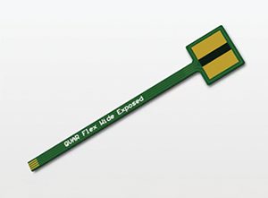
A typical Qvar electrode is shown in figure 1, which uses Q+ and GND pins to detect a charge variation, and enables the INT2 interrupt to rise when Qvar detects the presence of the human body in contact with the electrode. It is printed on a flex board with the contact surfaces (in copper) exposed. In this way, to detect a touch gesture, it can be put in the area of the device that should be touched by the user. The goal of the design is to let the user touch both the Q+ and GND area at the same time. For this reason, many different designs are possible. The exposed copper areas at the tip of the board are the actual electrodes. When both electrodes are touched, the sensor measures a high charge variation, and the output signal is almost saturated. This saturated signal is comparable to the press of a button.


© Technews Publishing (Pty) Ltd | All Rights Reserved
 printer friendly version