


Electronic circuits are becoming ubiquitous in modern life. Everywhere one looks, more and more processes that were once isolated and manual in nature, are being automated and now connected as the Internet of Things (IoT) becomes more established. The result is that electronic circuitry is progressively being positioned in increasingly hostile working environments, from cars, refrigerators and mobile devices to aircraft flight-control hardware, and is required to do more, faster, and in the smallest and lightest possible form factor.
In many cases, failure of the circuitry is inconvenient at best and expensive at worst. However, increasingly, as the infrastructure becomes ever more interconnected, individual failures will put the system at risk, which in turn may put lives in jeopardy.
Conformal coating is one technology that has been used to increase the reliability of electronic circuit boards operating in harsh environments over the last 50 years. Conformal coatings are thin, protective polymeric coatings, that are applied to protect the metal surfaces from corrosion, condensation, dielectric breakdowns and mitigate against tin whisker formation and conductive metal particles.
Traditionally, these materials have been furnished in solvent-based form, resulting in low-viscosity, easy-to-use materials. However, the use of solvents has become more restricted from an environmental point of view and consumers are increasingly becoming aware of the ‘waste’ of these processes in the form of the energy required to remove the solvents, as well as the impact of their release on the environment. Solvent-free technology is continually being requested more, essentially based on ethics, performance and process.
Ethically, solvent-free materials are a smart choice. They contain no solvents, so solvent emissions from your facility will be much lower. Depending upon local, regional and national legislation, this translates into cost savings due to simplified compliance with legislative requirements. The materials are non-flammable and are generally a much lower hazard to human health, resulting in potential cost savings on insurance. Often, the energy demands required for curing these materials are significantly lower than for solvent-based materials, resulting in reduced energy bills and reduced CO2 emissions.
From a performance point of view, solvent-free materials are generally applied slightly more thickly, resulting in increased coverage, and thus greater protective capability. The formulations are inevitably also more modern and deliver improved capability to meet the increased protective demands of new applications, e.g. automotive industry thermal shock cycling or aerospace increased condensation resistance.
In terms of process, modern materials are formulated to enable more rapid achievement of protective properties. Whether by condensation, UV, chemical curing mechanisms or a combination, modern materials are designed to improve manufacturing velocity and throughput. Being more modern, obsolescence of material capabilities is likely to be significantly further into the future than solvent-based vintages, which will only become harder to use and fall further behind the required protective capabilities demanded of modern assemblies.
UV curable coatings
UV curable materials cure extremely rapidly (seconds) when exposed to UV radiation of a suitable wavelength and intensity, making them an extremely interesting technology for increasing factory throughput and reducing production footprint. UV curable materials generally provide good protective properties and can provide improved chemical resistance compared with other cure types. UV curable materials have been used industrially in printing since the 1960s and this technology was transferred to the electronics industry in the 1980s, with the emergence of the first generation of UV curable conformal coatings.
Unfortunately, light only travels in straight lines and curing is line-of-sight only. Due to the 3D nature of a printed circuit board, it is entirely probable that some areas of the board will not achieve full exposure to the light, particularly material on the backside of component leads and beneath components. For this reason, UV curable materials need to contain a secondary cure mechanism, which can take the form of moisture, chemical or heat-based mechanism.
Moisture curing has traditionally been favoured because it requires no additional processes. However, in this case, the material is generally well cured in light exposed areas, thus increasing the difficulty of the diffusion of moisture into the coating and the emission of the leaving groups (commonly carbon dioxide).
The better the coating barrier, the longer the secondary curing process, and many days, weeks, months and even years have been reported.
When observing the infrared spectra of a leading UV/moisture cure material over time, an isocyanate peak took 93 days to disappear when stored at 23°C, 50% RH, indicating that the material took more than three months to reach its final properties. If we consider material beneath a component that does not see any UV exposure and is completely reliant on the secondary cure process, then it is clear that this could take even longer.
Heat activated secondary curing processes require additional processes and time, thus largely eliminating the benefit of the rapid primary cure. Speaking of which, the initial rapid cure can generate significant levels of stress, and seldom leads to more than 70-80% of the theoretical conversion to polymer, meaning that the materials can contain reactive groups that remain dormant. Once exposed to high temperatures (100°C and above) additional polymerisation can take place, resulting in the materials continuing to harden, change properties with time and be more prone to cracking during thermal shock transitions.
Materials containing a chemical secondary process, however, will cure completely within 6-8 hours at room temperature after exposure to suitable long-wavelength UV light (LED 365 nm, or iron doped ‘D’ bulb). The isocyanate peak has completely disappeared within six hours.
Due to the unique formulation of these materials, residual stress is minimised and the cure proceeds to a very high level of conversion, resulting in minimal changes in properties during thermal ageing.
In order to assess the changes in physical properties of the materials due to the thermal ageing process encountered in typical thermal shock experiments, sheets of the materials under test were moulded and cured with the recommended UV wavelengths and dose.
These sheets were then removed from the Teflon mould and die-cut into ‘dogbones’ and allowed to cure for 60 days at ambient conditions (25°C/45-55% RH). Five dogbones for each material were then tested for elongation and elastic modulus at -40°C, -20°C, 0°C, 20°C, 60°C, 100°C and 130°C. The results were consistent.
When we profile the elastic modulus and elongation at break, both key indicators of thermal shock performance, then these changes in the material properties after thermal ageing become apparent.
Looking at a conventional UV/moisture material, there is clearly a significant decrease in the overall elongation at break of the material, with the maximum value moving from about room temperature to somewhere around 100°C, showing that the material has further cross-linked during the thermal ageing and become more brittle.
For a typical chemical cure material, there is an overall net gain in elasticity and a greatly reduced shift in maximum elasticity from about 0°C to 20°C. In general the profile is similar and there is not much divergence in behaviour, showing that the material hasn’t changed much during the thermal ageing process, remaining elastic and flexible.
For a conventional UV/moisture cure material, there is a clear increase in the elastic modulus, indicating an increase in stiffness and a large increase in the stress applied to solder joints over a wider range, whereas for a chemical cure material, the elastic modulus remains constant during ageing.
A general note about the results shows that the conventional materials tend to be very stiff and inelastic at sub-ambient temperatures, whereas the chemical cure system remained elastic until -20°C, but still retained a degree of elongation even at -40°C.
Coefficient of thermal expansion (CTE) and glass transition temperature (Tg)
In addition to the modulus and elongation numbers shown, the CTE value and Tg are important numbers, which dictate the damage done to solder joints during thermal excursions, and the mismatch between the CTE of the assembly (5-15 ppm) and the coating (hundreds of ppm or more) are at least part of the reason why coatings crack during thermal shock testing.
The CTE values of a variety of coatings were measured by digital image correlation (DIC), a highly accurate optical measurement methodology. This measurement methodology is especially suitable for coating materials, where conventional TMA (thermal mechanical analysis) methods can be inaccurate due to sample softening. The sample sheets were produced, cured and aged alongside those used for producing the dogbones for the elongation and modulus study. The results of the DIC work are shown in Table 1. CTE1 is the CTE in the region below the Tg and CTE2 is the CTE value recorded above Tg.
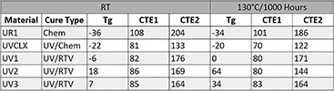
This data highlights that not only does the Tg of the various films increase with ageing (to a greater or lesser extent), but that there is a corresponding reduction in CTE during the ageing process, again to a greater or lesser extent.
The UV/moisture cured materials showed a greatly increased shift in Tg and larger changes in CTE, especially in CTE2. This indicates that the material is becoming increasingly cross-linked during thermal ageing, which again is consistent with the elongation and modulus data shown previously. Whereas, the chemical and UV/chemical materials showed a much smaller change in properties, again in line with the previous data.
Thermal shock testing
Whilst the lack of changes in physical properties during thermal ageing are an important parameter in material selection, the key to performance in an end-user application is whether a material can survive the required thermal shock profile without cracking or imparting additional stress on the solder joints.
In order to investigate this, 12 automotive engine control units (ECU) were selectively coated at a normal thickness with each of the five coatings in test. Four boards were subjected to a full thermal shock experiment from -40°C to +130°C, four boards were subjected to a 0°C to 130°C thermal shock regime, and the remaining boards were subjected to a -40°C to ±60°C thermal shock regime. After 250 cycles of each test cycle the boards were visually inspected for evidence of cracks in the coating, and the results are summarised in Table 2. The results were summarised using the following evaluation criteria:
0 – no cracks present
1 – cracks present on less than 5% of components
2 – cracks present on 5-10% of components
3 – cracks present on 11-15% of components
4 – cracks present on 16-20% of components
5 – cracks present on more than 21% of components
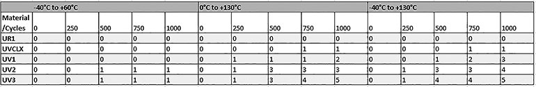 Table 2. Summary of coating thermal shock performance.
The most striking observation from this experimental work was that there was so little cracking in the boards that were subjected to the -40°C to +60°C cycle, and so little difference between boards that had been through the other shock regimes.
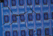
However, one thing was very clear: the materials which had the most stable properties during the thermal ageing process, the chemical cure and UV/chemical cure materials, exhibited very little cracking during the thermal shock experiment. UV1, which had the most stable thermal ageing properties of the conventional UV/moisture cure materials, exhibited a much lower level of cracking than UV2 and UV3 (the latter of which are shown in Figure 1).
Conclusion
The UV/chemical cure mechanism can be shown to be complete within six hours (to the limit of detection by IR spectroscopy) vs. the extremely long time required to complete the UV/moisture cure mechanism, which was greater than three months on a glass slide.
The UV/chemical cure material had significantly enhanced stability of the key physical properties during thermal ageing when compared to the conventional UV/moisture cure materials. This enhanced property stability led to a significantly improved thermal shock performance when compared to the established UV/moisture cure materials.
| Tel: | +27 11 454 8053 |
| Email: | [email protected] |
| www: | www.vepac.co.za |
| Articles: | More information and articles about Vepac Electronics |


© Technews Publishing (Pty) Ltd | All Rights Reserved
 printer friendly version