Additively manufactured electronics is an emerging approach that takes printed electronics into the third dimension. Printing both structural material and conductive traces offers benefits that include extensive design freedom, rapid development iterations, and more compact devices. IDTechEx divides the sector into two aspects: ‘fully additive’ and ‘printing onto 3D surfaces’. Both have multiple application opportunities that IDTechEx believes will develop over the next decade.
Fully additive electronics manufacturing
If both structural and electronic aspects of a component are printed, then the manufacturing process can be regarded as ‘fully additive’. This manufacturing approach provides a lot of freedom since there are no constraints on how the conductive traces are distributed within the printed structural dielectric. This enables features such as helical antenna, integrated capacitors, and ramped vias that are challenging or impossible to produce with conventional methods.

Furthermore, SMD components can be incorporated within the structure if desired.
Applications of fully additive electronics manufacturing include circuit prototyping, since complex multilayer circuits can be produced in-house far more quickly than sending the designs to an external prototyping house. Another promising application with a potentially huge market is advanced electronics packaging, in which bare dice are embedded within a printed structure that contains fine electronic traces. An advantage of this approach over conventional electronics packaging is that silicon ICs can be placed closer together, making the entire system more compact.
Printing onto 3D surfaces
Additively manufactured electronics can also include applying electronic functionality to existing 3D surfaces. For example, conductive tracks could be printed onto an injection-moulded plastic part using methods such as aerosol printing or material extrusion. Durability and robustness can then be improved by printing a dielectric material over the top. Furthermore, SMD components can be mounted onto the 3D surface using pick-and-place and conductive adhesives. This approach has a lot of promise for adding electronics to larger parts, where the time to print the structural plastic would be prohibitive.
A key target application for this approach is replacing wiring in consumer products, vehicles, and even aircraft. At present, installing wiring is a laborious manual task, with the potential for mistakes and subsequent short circuits if wires rub against each other. Printing the wiring directly onto a 3D plastic surface enables the process to be automated and increases durability, as the conductive traces are ultimately embedded within a dielectric material.
Incorporating microfluidics and photonics
As additive electronics manufacturing becomes more established, an increasing range of functionalities is likely to be incorporated within the additively manufactured component. This could include microfluidics, with electrical sensors, piezoelectric actuators, and even other MEMS components embedded within a 3D, predominantly plastic item. Labs-on-a-chip for medical diagnostics and wearable sensors for sweat analysis are both promising applications.
Additively manufactured electronics are also compatible with photonic structures, although this will generally require improvements in the printing resolutions of both the dielectric and conductive elements. Example potential applications include photonic sensors, in which the refractive index of an optical path is changed by temperature or gas absorption, and ultimately optoelectronic components.
Adoption roadmap
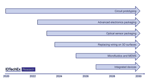
Considering the current stage of development, and the additional requirements such as manufacturing throughput and resolution, Figure 1 shows a roadmap for a range of additively manufactured electronics applications. Circuit prototyping is already commercialised, while integrated devices with many different functionalities are likely to be the most challenging to develop.
To learn more about the opportunities for additively manufactured electronics featured in this article, from both a technical point of view and in terms of market size and forecast, see the IDTechEx report ‘3D Electronics 2020-2030: Technologies, Forecasts, Players’ (accessible via the short URL www.dataweek.co.za/*mar21-idtechex).

© Technews Publishing (Pty) Ltd | All Rights Reserved