


![]()
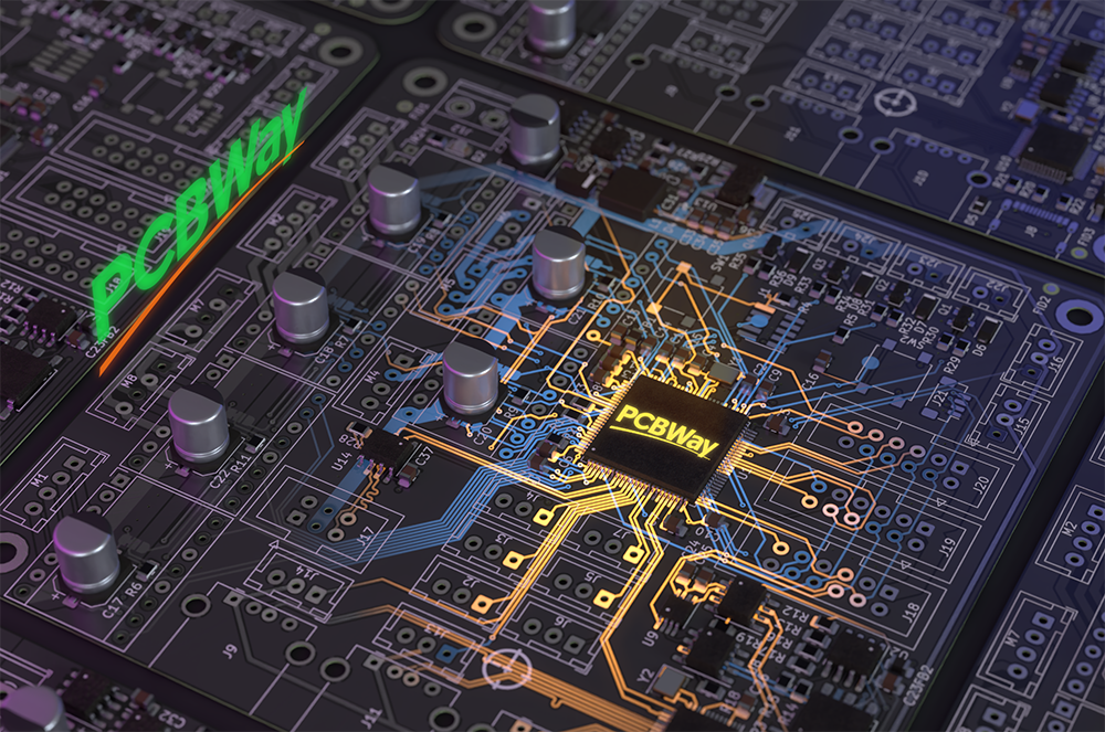
[Sponsored] In the digital era, AI and big data technologies are developing at a rapid pace. PCBWay is continuously advancing its PCB manufacturing technology to support the growth.
Industry landscape and demand data
According to the International Data Corporation (IDC), the global AI server market reached $30,7 billion in 2023, marking a year-over-year growth of 35,6%. Among these, cluster servers used for training large AI models place particularly demanding requirements on hardware – each GPU node requires an ultra-high-performance motherboard. Big data analytics is also fuelling demand. According to global data platform Statista, the total volume of global data reached 120 ZB (1 ZB = 1 billion TB) in 2023. Cloud computing giants like Amazon AWS are deploying servers by the millions.
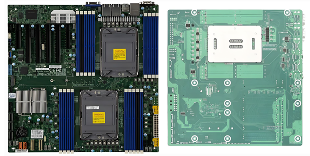
At the heart of all this lies the server motherboard – regarded as the ‘brain’ of AI systems – making the PCB substrates that support AI computing the lifeline of the electronics industry. These motherboards must host high-speed chips and ensure real-time processing of massive data volumes.
Manufacturing challenges and key technical requirements
However, the design and manufacturing of such PCBs come with extremely high technical barriers; they typically require 18+ layers, 4-8 step HDI (High Density Interconnect) structures, and must use high-frequency, high-speed base materials.
• Interlayer alignment and lamination control: PCBs with more than 18 layers require three or more lamination cycles, making them highly susceptible to layer misalignment, which can result in short circuits.
• Microvia technology: Laser drilling must penetrate via diameters of 2-4 mils, which often leads to issues such as ‘taper defects’ and ‘pad separation’, both of which negatively affect conductivity.
• Signal integrity: At high frequencies, the skin effect becomes more pronounced, requiring gold surface finishes (electroless nickel immersion gold combined with electroplated nickel-gold) to ensure impedance stability. The main challenge lies in achieving uniform plating, with a variation tolerance of ±0,05 μm.
• Thermal management of materials: High-frequency PCB materials must have a coefficient of thermal expansion (CTE) that matches copper (16 ppm/37℃); otherwise, the risk of delamination during high-temperature reflow soldering increases by 40%.
PCBWay’s achievements
As a leading company with a decade of experience in HDI PCB manufacturing, PCBWay has been focusing on high reliability and high-precision production since 2014. We have continuously advanced our technology in small-batch HDI PCB manufacturing, gradually bridging multiple technical gaps in complex HDI PCB processes.
Focusing on the niche field of server motherboards, PCBWay has established four core technical pillars: fine trace technology, interlayer alignment, microvia fabrication, and signal integrity control.
In 2023, PCBWay successfully broke through the engineering prototype process for 8-step HDI PCBs. In 2025, we achieve mass production of 8-step HDI boards, with 12-step HDI technology already under preliminary research for 2028.
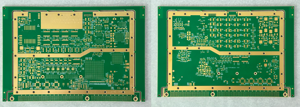
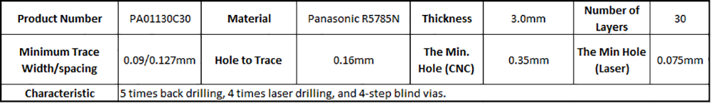
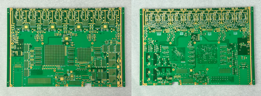
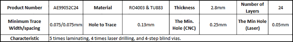
Below are some sample server-grade PCBs developed by PCBWay:
For every 1% growth in the AI server market, millions of high-performance PCBs are required. PCBWay promises to continue filling this gap and accelerating innovation by using technology-driven solutions. At the same time, we invite global partners to join us on this journey, turning every engineering prototype and small-batch server motherboard into a spark that drives the intelligent world forward.
| Tel: | +86 571 8531 7532 |
| Email: | [email protected] |
| www: | www.pcbway.com |
| Articles: | More information and articles about PCBWay |


© Technews Publishing (Pty) Ltd | All Rights Reserved
 printer friendly version