


Since 'nothing solders like solder', HAL (hot air levelling) will continue to hold a significant place in the surface finishing industry. Furthermore, the wave soldering process will continue to be a viable means of electronics assembly. However, as automatic soldering processes using lead-free alloys have become increasingly prevalent, questions have arisen about copper dissolution into these alloys.
The Sn/Ag/Cu family of alloys is the leading candidate for a lead-free alternative. A study was conducted by AIM to determine if there is any significant difference between Sn/Ag/Cu alloys when used in automatic soldering equipment in terms of copper build-up in the system. The study compared two Sn/Ag/Cu alloys to determine if, at processing temperatures, one alloy would absorb less copper than the other alloy.
The second part of this experiment was to determine how to effectively control copper build-up in automatic soldering equipment.
Presently, manufacturers have been able to limit the copper in a solder bath by precipitating the copper out using a simple gravimetric separation of Cu6Sn5. Unfortunately, because the density of high-tin lead-free alloys is lower than that of Cu6Sn5, the Cu6Sn5 intermetallics sink and are dispersed through the lead-free alloy in the pot.
Therefore a procedure for separating copper intermetallics from lead-free pots has had to be developed. Yet another issue is that there is not yet an agreed upon industry specification for lead-free pot maintenance. Clearly, this will be needed as a guideline for the users of these alloys. To accomplish this, a specification is proposed based upon these experiments.
Copper dissolution in Sn/Ag/Cu alloys
The first part of this study was performed to determine if there is any significant difference between Sn/Ag/Cu alloys in terms of copper dissolution. The study compared Sn/Ag3/Cu0,5 (LF218) to Sn/Ag2,5/Cu0,8/Sb0,5. The purpose was to determine if, at wave soldering temperatures, one alloy will absorb less copper than the other alloy.
Test procedure</b>
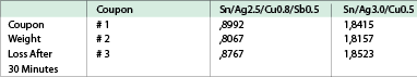
Two pots of each alloy holding approximately 500 grams of metal were heated to 276°C. Copper strips were weighed, fluxed and then placed into the lead-free alloys. The temperature and strips were monitored every 5 minutes for any visual change. After 30 minutes changes were noticed. The copper coupons were then removed and weighed.
Observation
As shown in Table 1, Sn/Ag3,0/Cu0,5 dissolves almost double the amount of copper as Sn/Ag2,5/Cu0,8/Sb0,5 does at the same temperature over the same short period of time. From this it is inferred that Sn/Ag2,5/Cu0,8/Sb0,5 is more stable in automatic soldering equipment and should require less initial alloy maintenance.
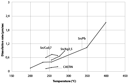
This result is corroborated by studies showing the lower copper dissolution of Sn/Ag2,5/Cu0,8/Sb0,5</sub> versus other lead-free alloys, as shown in Figure 1. It should also be noted that extensive third-party testing has demonstrated that this alloy is a viable choice for the HAL process, demonstrating good coverage and solderability with flatter pads than Sn/Pb.
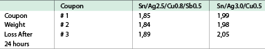
In order to determine the upper limits of copper contamination, the testing continued over a 24 hour period. The bath was subjected to excessive copper. As shown in Table 2, at the end of the second 24 hour period it was found that the Sn/Ag3/Cu0,5 and Sn/Ag2,5/Cu0,8/Sb0,5 absorbed very similar amounts of copper.
During this second 24 hour period the solder in the pots started to exhibit sluggish flow. The pots were then emptied and large amounts of Cu6Sn5 intermetallics were found at the bottom of each pot. This was a problem that had not been anticipated since with a standard Sn63/Pb37 wave pot the Cu6Sn5 will float and can be removed easily.
Controlling copper build-up
Different proposals have been suggested for lead-free wave soldering. One option is to use the Sn/Cu0,7 alloy for wave soldering and Sn/Ag/Cu for surface mount. However, this method is very difficult to control, inventory can be hard to manage and eventually the alloys would get mixed on the circuit board.
Another idea is to use a low silver (<3,0Ag) Sn/Ag/Cu alloy for all applications. A third is to use a high silver content (>3,8Ag) Sn/Ag/Cu alloy. Unfortunately, it appears that whichever process is implemented, wave solder pot maintenance could be problematic.
Copper is a well-understood contaminant in the Sn63/Pb37 alloy for automatic soldering applications. If the copper level in pots becomes too high, the solder may suffer from poor flow as well as experience embrittlement issues.
In a standard Sn63/Pb37 wave pot, as impurities such as copper build up, these form intermetallics with the tin. This intermetallic build up can be systematically removed by reducing the temperature of the solder pot to 188°C and allowing the pot to sit undisturbed for more than 8 hours.
The density of the Cu6Sn5 intermetallic is 8,28, while Sn63/Pb37 is 8,80, allowing most of the Cu6Sn5 to float to the top of the pot after a few hours of cooling. After this the top of the pot is skimmed and new solder is added to bring up the level.
This typically will maintain copper levels below 0,3% and can maintain the copper level in the 0,15% range. This is a simple gravimetric separation of Cu6Sn5.
Unfortunately, whether Sn/Cu or Sn/Ag/Cu is implemented for wave soldering, the density of both alloys is less than Sn63/Pb37. The densities for these lead-free alloys are approximately 7,39, versus 8,80 for Sn63/Pb37 and 8,28 for Cu6Sn5.
Therefore, instead of the intermetallics floating off and easily being removed as with Sn63/Pb37, the intermetallics sink and are dispersed through the lead-free alloy in the pot.
To add to this problem, in the case of lead-free electronics assembly, more organic coated (OSP) copper boards are utilised. This will result in more copper exposure to the wave, and eventually these intermetallics could build to a point where they plug the wave pump’s baffles.
The result and biggest problem of all of the above is that solder pots may need to be dumped more often, leading to a complete changeover of the wave pot. The pot dump specification will most likely be around 1,55% copper, since above this point the alloy becomes sluggish and at 1,9 to 2% precipitation in the pot starts to occur, which can lead to damage to the wave pump and baffles.
Yet another issue is that there is not yet an agreed upon industry specification for lead-free pot maintenance. Clearly, this will be needed as a guideline for the users of these alloys. Therefore, the chart shown as Table 3 has been developed from empirical studies and metallurgical evidence.
Although separating the copper intermetallics from lead-free pots is more complicated than when using Sn/Pb, it is still achievable. To do so, a second pot capable of holding the volume of alloy from the HAL machine should be used.
This should be a round bottom pot open to the atmosphere, preferably with a beach built into the top lip of the pot. This beach allows the crystalline structure that works like a sponge to allow the alloy to drain back to the pot.
The first step when separating the copper intermetallics from lead-free pots is to transfer the used alloy into the second pot at an elevated temperature (400°C). After the solder is transferred, the pot should be cooled to 260°C. At this point, precipitate will form at the bottom of the pot.
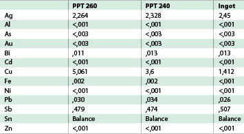
A ladle with holes in it or a rake that can pull the material up onto the beach on the sidewall of the pot should be used to remove this precipitate. At this point a sample of the precipitate should be removed and labelled as ‘PPT 260’. Then, the pot should be further cooled to 240°C and a sample of the alloy cast into ingot form and labelled as ‘Ingot’.
At this point, there will be more precipitate in the bottom of the pot, and this should also be removed and a sample of it labelled as ‘PPT 240’. Then, all three samples should be sent to a laboratory for analysis. These actions should reduce the copper content of the existing solder back to an acceptable level of 1 to 1,4%. Table 4 shows the results of the analyses on these materials.
Results and conclusion
As demonstrated, by cooling the pot and removing the precipitate the copper level was lowered down to an acceptable level. Therefore, it is possible to salvage lead-free solder using a similar method as used with Sn/Pb, except that the SnCu intermetallics now sink instead of float, and instead of being skimmed now need to be dragged from the bottom of the pot.
The end result is that copper levels can be reduced in a lead-free soldering pot to within acceptable levels.
| Tel: | +27 31 822 8555/6 |
| Email: | [email protected] |
| www: | www.truthelectronics.co.za |
| Articles: | More information and articles about Truth Electronic Manufacturing |


© Technews Publishing (Pty) Ltd | All Rights Reserved
 printer friendly version