13 July 2016Manufacturing / Production Technology, Hardware & Services
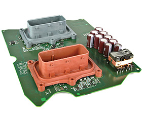
The X-ray inspection system X Line 3·D from Göpel Electronic enables reliable inspection of THT and pin-in-paste solder joints in compliance with the IPC quality standard, through a unique combination of 3D X-ray (AXI) and 2D AOI inspection.
That is particularly important for automotive assemblies which are subject to strict quality requirements.
Unlike simple two-dimensional X-ray inspection, 3D X-ray inspection allows evaluation of the solder penetration for THT connectors. Assemblies which are subject to the IPC norm must show a solder penetration of 50 to 75% at the pin, depending on the IPC class. These requirements can be assured through evaluation of the solder penetration layer by layer.
The limits of X-ray technology in this particular application are, however, the requirement of circumferential wetting of pins and the wetted connecting surface (ring). As an example, according to IPC, the circumferential wetting must be proven to be between 270° and 330°. Only the combination of two technologies can provide compliance with this standard. By using a fully integrated and automated AOI module, both circumferential wetting and wetted connecting surface can be evaluated at the solder side.
With the X Line 3·D and the AXOI technology (combined X-ray and optical inspection), maximum fault coverage at line cycle times can be achieved. By scanning image acquisition, time-efficient quality control is made possible. Hole fill levels, pin and pad wetting, bridging and solder balls can be detected with this single system.
The machine is an inspection system for the safe testing of double-sided assembled PCBs. The three-dimensional X-ray inspection covers both top and bottom sides within a continuous process. The basis of this technology is real-time, multi-angle image acquisition, which allows a complete 3D capture of the assembly. Integrated reconstruction methods based on planarGT provide detailed evaluation of the PCB under test, layer by layer.
World-first 016008 mm component placement
Manufacturing / Production Technology, Hardware & Services
Fuji has achieved the world’s first placement of 016008 mm (0,16 x 0,08 mm or 006 x 003 inches) size components on printed circuit boards with its SMT pick and place machine, NXTR.
Read more...Lifecycle and obsolescence: Protecting electronics through process Production Logix
Manufacturing / Production Technology, Hardware & Services
At Production Logix, we believe longevity is not accidental. It is engineered through early visibility, structured response, and disciplined execution, in partnership with our OEM customers.
Read more...Maximising squeegee quality and durability Testerion
Manufacturing / Production Technology, Hardware & Services
Transition Automation has announced two new product advancements designed to improve SMT printing performance and extend squeegee life: laser-enhanced Permalex bonding and integrated edge protectors.
Read more...NeoDen ND2 PCB screen printer ZETECH ONE
Manufacturing / Production Technology, Hardware & Services
The NeoDen ND2 PCB screen printing machine is a fully automatic stencil printer designed to deliver precise and consistent solder paste application in modern SMT production environments.
Read more...Understanding the BGA rework process Techmet
Manufacturing / Production Technology, Hardware & Services
BGA rework is a highly technical process that involves removing the faulty component, preparing the circuit board, and installing a new or repaired device, while maintaining the integrity of the printed circuit board.
Read more...Flexible three-process reflow soldering system Truth Electronic Manufacturing
Manufacturing / Production Technology, Hardware & Services
By combining multiple soldering technologies within a single system, the Vision TripleX system enables manufacturers to adapt easily to different assembly requirements, board designs, and production volumes.
Read more...Inline vapour phase soldering for high-volume production MyKay Tronics
Manufacturing / Production Technology, Hardware & Services
The VP2200-100 vacuum inline vapour phase soldering system from ASSCON is designed for fully automated, high-volume electronics manufacturing where process consistency and solder joint quality are critical.
Read more...Global electronics solutions since 1964 IMP Electronics Solutions
Manufacturing / Production Technology, Hardware & Services
Over more than six decades, IMP Electronics Solutions has built a reputation for technical expertise, reliable supply chains, and strong partnerships with both customers and manufacturing partners.
Read more...Driving excellence in electronics manufacturing Jemstech
Editor's Choice Manufacturing / Production Technology, Hardware & Services
Jemstech’s reputation for disciplined execution and client-focused service has earned it strong loyalty from companies operating in demanding industries.
Read more...When do you need Nitrogen in reflow? Truth Electronic Manufacturing
Manufacturing / Production Technology, Hardware & Services
Nitrogen in reflow soldering is often seen as a performance enhancer, offering improved wetting, shinier joints, and fewer defects. But it is not always necessary.
While every effort has been made to ensure the accuracy of the information contained herein, the publisher and its agents cannot be held responsible for any errors contained, or any loss incurred as a result. Articles published do not necessarily reflect the views of the publishers. The editor reserves the right to alter or cut copy. Articles submitted are deemed to have been cleared for publication. Advertisements and company contact details are published as provided by the advertiser. Technews Publishing (Pty) Ltd cannot be held responsible for the accuracy or veracity of supplied material.


 printer friendly version