


In the ongoing quest to discover the next wonder material that will push the limits of semiconductor technology beyond the fundamental physical limitations of silicon, graphene has received the most attention over the past several years. While research is also underway on several other alternatives, black phosphorus is emerging as a strong contender.
Graphene has many extraordinary properties, chief among them its strength (roughly 200 times stronger than steel), highly efficient conduction of electricity and heat, as well as being almost transparent. Its energy efficiency is primarily a result of its one-dimensional nature i.e., it is only one atom thick.
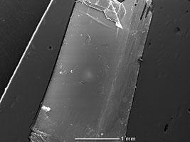
Now, it has been shown that ultra-thin layers can also be formed by black phosphorous. Chemists at the Technical University of Munich (TUM) have now developed a semiconducting material in which individual phosphorus atoms are replaced by arsenic. Like graphene, which consists of a single layer of carbon atoms, black arsenic phosphorus forms extremely thin layers. The array of possible applications ranges from transistors and sensors to mechanically flexible semiconductor devices. Unlike graphene, whose electronic properties are similar to those of metals, black arsenic phosphorus behaves like a semiconductor.
A cooperation between the Technical University of Munich and the University of Regensburg on the German side, and the University of Southern California (USC) and Yale University in the United States, has for the first time produced a field effect transistor made of black arsenic phosphorus.
The new technology developed at TUM allows the synthesis of black arsenic phosphorus without high pressure; this requires less energy and is cheaper. The gap between valence and conduction bands can be precisely tuned by adjusting the arsenic concentration. “This allows us to produce materials with previously unattainable electronic and optical properties in an energy window that was hitherto inaccessible,” says Professor Tom Nilges, head of the research group for Synthesis and Characterisation of Innovative Materials.
With an arsenic concentration of 83% the material exhibits an extremely small band gap of only 0,15 electron volts, making it predestined for sensors which can detect long wavelength infrared radiation. LiDAR (Light Detection And Ranging) sensors operate in this wavelength range, for example. They are used, among other things, as distance sensors in automobiles. Another application is the measurement of dust particles and trace gases in environmental monitoring.
A further interesting aspect of these new, two-dimensional semiconductors is their anisotropic electronic and optical behaviour. The material exhibits different characteristics along the x- and y-axes in the same plane. To produce graphene-like films the material can be peeled off in ultra thin layers. The thinnest films obtained so far are only two atomic layers thick.
In another study published in Nature Communications, scientists from McGill University and Université de Montréal reported that when electrons move in a phosphorus transistor, they do so only in two dimensions. “Transistors work more efficiently when they are thin, with electrons moving in only two dimensions,” explains Thomas Szkopek, an associate professor in McGill’s Department of Electrical and Computer Engineering and senior author of the new study. “Nothing gets thinner than a single layer of atoms.”
The black phosphorus studied in this research is a form of phosphorus that is similar to graphite and can be separated easily into single atomic layers, known as phosphorene. Phosphorene has sparked growing interest because it overcomes many of the challenges of using graphene in electronics. Unlike graphene, which acts like a metal, black phosphorus is a natural semiconductor – it can be readily switched on and off.
“To lower the operating voltage of transistors, and thereby reduce the heat they generate, we have to get closer and closer to designing the transistor at the atomic level,” Szkopek says. “The toolbox of the future for transistor designers will require a variety of atomic-layered materials: an ideal semiconductor, an ideal metal and an ideal dielectric. All three components must be optimised for a well designed transistor. Black phosphorus fills the semiconducting material role.”
To examine how the electrons move in a phosphorus transistor, the researchers observed them under the influence of a magnetic field in experiments performed at the National High Magnetic Field Laboratory in Florida, the largest and highest-powered magnet laboratory in the world.
“What’s surprising in these results is that the electrons are able to be pulled into a sheet of charge which is two-dimensional, even though they occupy a volume that is several atomic layers in thickness,” Szkopek says. That finding is significant because it could potentially facilitate manufacturing the material.






© Technews Publishing (Pty) Ltd | All Rights Reserved
 printer friendly version