


We see third-generation I/O (3GIO) serial connectivity standards showing up everywhere: HyperTransport, InfiniBand, and PCI Express. Why are all the major platform vendors moving to these new interconnect schemes? Basically, the speed of this 'serial tsunami' is being driven by the inability to cost-effectively resolve signal and power integrity issues prevalent in standard synchronous, parallel, multidrop bus designs.
Power and ground noise due to large high-frequency current demands in large voltage swing, single-ended designs; reflections from stubs due to multidrop connections; impossible delay/skew constraints for data versus clock nets; and other limitations, have made cost-effective highspeed parallel design unattainable.
At the crest of the serial tsunami are differential signalling, embedded clocks, pre-emphasis, and point-to-point interconnect - all these elements give us a way around the electromagnetic barriers of parallel multidrop design. These changes require us to change our verification methodologies to assure successful designs. Let us take a look at some of the changes in detail, focusing on how they affect the need for up-front planning and verification.
Differential signalling
Low voltage differential signalling (LVDS) is the real basis for the transition to 3GIO. LVDS, a two-wire system where return currents are expressly dealt with by the second closely coupled wire, is used to minimise ground-return loops and the cumulative effect produced by wide parallel buses on that return loop (otherwise known as simultaneous switching noise, or SSN). At these high frequencies, though, it is still very important to maintain a complete ground return path (no cuts or voids in the ground plane), especially for common mode currents.
New 3GIO constraints for differential (diff) pair topologies include:
* Minimise coupling from adjacent pairs.
* Match length of traces in a pair.
* Minimise the number of vias used, but match use and location within pairs when they are used.
The idea here is that the more the diff pair is coupled, the more external noise will be rejected. An aggressor pair will induce a signal in the victim pair, but as such, it would induce the same signal in both wires (if they are closely coupled). Any noise agent that affects both wires in a diff pair will have no effect on the resulting differential waveform.
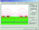
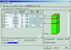
So, it is important that a verification tool understands the self-coupling of each diff pair and the coupling between pairs, including broadside (up and down a layer) and edge-coupled (side to side on same layer) pairs. Figure 1 shows the EM field lines calculated by the Mentor Graphics HyperLynx 2D field solver for two diff pairs. Notice the difference in the number of lines (which indicate field strength) between members of a pair versus those between the pairs themselves. Impedance planning is an important step with diff pairs where internal terminations might require you to maintain specific differential impedance. For this reason, we have included an impedance-planning dialog in the HyperLynx stackup editor, as shown in Figure 2. In the editor, one can simply set a priority parameter, such as trace width, and request a spacing value that allows one to reach a goal (say, a differential impedance of 100 Ω).
Vias
At extremely high frequencies, using vias can increasingly introduce signal integrity (SI) problems. Why? Vias are a discontinuity in the transmission line.
Just visualise the nicely-controlled impedance of a trace over a ground plane and then compare that to a vertical tube of copper with no corresponding ground return path - the impedance is clearly different. In these systems, it is important to keep diff pair vias close together and to add ground stitching vias in the vicinity for shielding and common mode return.
However, it is also important to simulate the impedance discontinuity. HyperLynx Version 7.0 has given you the ability to have via L and C calculated automatically, to specify L and C values for each via type, or to set a default via value for the entire board.
Transmission line losses
Without going into a lengthy discussion on losses in transmission lines, let us just stress the importance of your verification and planning tools in recognising and supporting loss. As frequencies increase, AC losses are significant. Skin effect (where more current is forced to the surface of a conductor) and dielectric loss (thermal heating of the dielectric as the EM waves travel through the dielectric) are the culprits. Especially in backplanes where the trace length on FR4 can be substantial, losses will reduce and 'smear' voltages at the receiver. This reduces your ability to have a clean 'eye' for the receiving IC to sync to, and extract, the correct data. HyperLynx Version 7.0 includes the trusted 'W' element in its simulator for robust loss support.
High-speed models
Modelling and simulation go hand-in-hand. Whether you are doing analog or digital simulation, you cannot get very far without models. In the SI business, the I/O buffer information specification (IBIS) standard has been a huge benefit to systems designers. Virtually all IC vendors are now making I/O models available for their devices.
As we enter this next decade with 3GIO, IBIS is moving to support subcircuit models in SPICE (simulation program with integrated circuit emphasis) or VHDL_AMS in the proposed IBIS 4.1 (now Bird 75) specification. In the meantime, simulation environments must support the models that are currently available, and those are predominately HSPICE (from MetaSoft).
HyperLynx Version 7.0 offers support for HSPICE models. These models are generally encrypted and require a licence for the HSPICE simulator; Version 7.0 calls the HSPICE simulator from the HyperLynx environment. Model assignment and waveform analysis are the same as always, but behind the scene HyperLynx prepares a SPICE netlist of the entire electrical topology (including all coupling and loss elements) and then invokes HSPICE, extracts the results, and presents them in the native HyperLynx environment. This includes any multibit stimulus patterns you have defined.
For example, if you want to simulate a Xilinx RocketIO multigigabit transceiver implementation, simply assign the RocketIO model just as you would an IBIS model and use either your true topology extracted from your layout system (HyperLynx supports trace model extraction from all major PCB vendors) or a 'what-if' topology defined in HyperLynx. Then hit the simulate button and view the results that are displayed in an eye diagram based on HSPICE results.
Eye diagrams
For us digital designers, an eye diagram - as shown in Figure 3 - is nothing more than what we have been used to looking at in a logic analyser for years - data bits and high and low voltage levels. The difference between a logic analyser and an eye diagram is that in the eye, hundreds of bits are overlaid on each other so that we can see if there is a large enough window of time where the signals are reliably in one state or the other (necessary for the receiver clock recovery circuit to dependably extract the data).
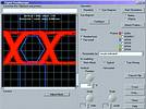
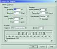
As in digital simulation, we are required to create stimuli that can affect the signals in a realistic way, which in turn we see as a changing shape in the 'eye'. Because the bit history will affect the analog result, an easy-to-use multibit stimulus editor in HyperLynx Version 7.0 has been added that allows you to create bit streams of ones and zeros for the simulator to drive the diff pair (Figure 4). Pseudorandom, 8-bit/10-bit encoded and customer defined patterns are supported, as well as random (uniform or Gaussian) jitter. This functionality, combined with easy-to-use differential probes, provides you with robust eye diagram support.
3GIO systems typically specify what a sufficient eye should look like for a receiver to extract the clock and data. This capability is referred to as an 'eye mask'. The ability to specify an eye mask is included in HyperLynx Version 7.0, giving you an easy way to 'see' in the oscilloscope view if your resulting eye pattern meets the manufacturer's specification.
Conclusion
High-speed, low-voltage differential serial interconnect is the wave of the future for both interboard and intraboard interconnects. The features you need in a verification and analysis tool are changing to support this transition. Because tolerances are extremely tight in all aspects of these interconnect systems, the entire system must be simulated to assure first-pass success of the PCB design.
In summary, consider a quote from an Intel white paper on PCI Express, "...detailed simulation and validation are necessary to guarantee a successful design." We at Mentor Graphics believe our latest release of the HyperLynx products will make this task easier and more productive. We wish you luck as you move into the gigahertz world of serial connectivity.
ASIC Design Services is holding free seminars on PADS PCB and Hyperlynx Signal Integrity tools. For more information contact Kobus van Rooyen, 011 315 8316, [email protected]
| Tel: | +27 11 315 8316 |
| Email: | [email protected] |
| www: | www.asic.co.za |
| Articles: | More information and articles about ASIC Design Services |


© Technews Publishing (Pty) Ltd | All Rights Reserved
 printer friendly version