


One popular notion is to use lead-free solder as a way to eliminate one of the most harmful chemicals from manufacturing's outflow. Longer-term are the issues of safe lead disposal as landfills, incineration and other methods come under increasing scrutiny.
For the industry's part, perfecting the composition, application and reflow of lead-free solder represents a triumph over many technical obstacles across many scientific disciplines. However, the question remains: how does this affect the automated inspection systems developed for conventional lead-solder applications?
Why lead-free solder inspection is difficult
There are two characteristics of lead-free solder joints that make optical inspection challenging:
* The reflowed shape of the joints, a function of wettability, generally is uneven, prompting inconsistent inspections.
* Their surfaces tend toward dull, matte finishes.
There are three reasons for these characteristics:
1. Fillet-shape dispersion. Final fillet shapes depend on several variables, including circuit design, assembly-line conditions, various component-plating technologies, flux selection and wave-solder reflow temperature. Thus, as lead-free solder melts, the alloy's surface tension is stronger than that of conventional tin/lead (Sn/Pb) materials. The result is that it has more difficulty spreading along surfaces. Its capacity for soldering, or wettability, depends on its attraction to the land materials, ie, integrated circuit (IC)-lead plating, making fillet shape a factor of even more variability.
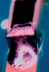
2. Matte solder surfaces. Eutectic Sn/Pb solder generally bears a reflective surface and appears smooth. In contrast, lead-free solder joints usually display a dull or matte surface that looks rough (Figure 1). This is because lead-free solder is a non-eutectic alloy. After reflow, it drops in temperature neither quickly nor uniformly. Generally, lead-free solder has a liquid- to solid-state temperature difference of about 10°C. Because of this slow cooling process, the metal composition starts to solidify non-uniformly such that the liquid and solid states coexist - the source of the dull surfaces. On the other hand, with quick cooling down periods, surfaces become comparatively smoother. In short, whether dull or shiny and smooth, much depends on the cooling temperature conditions. Moreover, the range of dull surface types varies widely.
3. Reflection characteristic of solder surfaces. There is a correlation between solder surfaces and their reflective characteristics, which depends on the time it takes the solder to solidify. An Sn/Pb solder fillet surface is smooth and its surface comparatively even, the conditions prompting a reflective surface. Occasionally, lead-free solder will exhibit a reflective surface similar to that of Sn/Pb solder only to become dull and non-reflective, depending on the cooling temperature conditions. When lead-free solder hardens and becomes totally non-reflective, it appears both dull and slightly white in colour.
Lead-free solder and automatic inspection
To an automated optical-based solder inspection system (AOI), the dull surface of a lead-free solder joint appears white or features a white mask that obscures the fillet's actual shape. However, new systems that use a colour-highlight technology have proven to be effective in overcoming reflection problems in inspection.
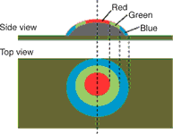
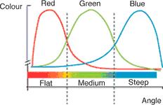
Colour highlighting, to inspect for solder quality, works by using a source to project red, green and blue lights onto a printed circuit board (PCB) surface at different predetermined angles. The camera 'captures' the colours as they reflect off the board, its components and solder, producing a 2D image that, nevertheless, conveys 3D information (Figure 2). The red colour reflects off near-flat surfaces; the green off medium angles and the blue off steep angles - all captured by the colour camera. In this manner, the colour-highlight system can process the reflective patterns to identify the solder shape, even if whitening masks it.
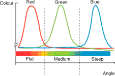
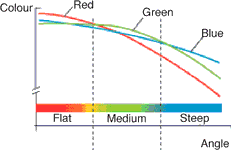
The colour-highlight system uses algorithms to convert the red flat angles, green medium angles and blue steep angles into a topographical 3D picture of the solder joint. Figure 3 graphically shows the distribution of colour information in RGB (red/green/blue) for the leaded-solder joint, lead-free solder joint and white diffusion board, respectively. In Figure 3a, the leaded-solder surface features sharp peaks for each of the colours, ie, the colour highlights are clear. In Figure 3b, however, the non-reflective, lead-free solder graph shape spreads and the ratio of mixed colour between R and G and between G and B is increased. However, the maximum values of each RGB remain the same, ie, the colour-highlight system is able to convert the colour to shape information. Finally, Figure 3c shows that, even with a white diffusion board, the colour-highlight system will pick up reflections that can be separated into maximum values of each RGB. Thus, even if the reflection is low, the correlation between the colour and the angle is the same and a fillet shape emerges.
'De-white' processing
Low reflection levels of lead-free solder surfaces challenge all AOI systems by appearing whitish in colour. If the white becomes stronger and the image more faded, it is difficult to program an inspection system for a lead-free soldered PCB. In response, an algorithm has been developed to 'de-white' the image and correctly amplify the colours for easier inspection programming and colour-image processing.
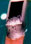
To study the whitish solder surface, the same solder shape is formed of both a reflective surface using leaded solder and a non-reflective surface using lead-free solder; both images are captured using the colour-highlight system (Figure 4). In the case of a reflective surface (Sn/Pb solder), a clear red colour appears in the centre whereas with a dull (lead-free solder) surface, a whitish colour appears instead of a vivid red.
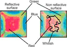
After measuring the pixel values out of the whitish area, each RGB colour is measured. As stated, a red typically appears in the whitish area. Hence, the ratio of red is greater than the other colours. However, the ratios of the green and the blue are of almost the same value, which provides the evidence to confirm fading to a whitish colour.


© Technews Publishing (Pty) Ltd | All Rights Reserved
 printer friendly version