


The globalisation of markets results in stronger competition with clearly noticeably cost pressure. For companies producing electronic equipment, it is therefore of extreme importance to reduce production costs whilst maintaining a consistently high quality level of the manufactured products. Manual repair soldering that is expensive, time consuming and cost intensive is already unacceptable due to the required quality and reproducibility of the whole manufacturing process.
In addition, densely populated multilayer boards and miniaturised, high-pin-count, fine-pitch devices cannot be efficiently repaired with high quality. Hidden costs, such as productivity rates, operator training and damaged assembly costs have to be taken into consideration as well. Special focus has to be put on lead-free applications, as manual repair soldering processes can cause enormous thermal problems.
The target, therefore, has to be a zero-fault selective soldering process.
An appropriate printed circuit board design is of the utmost importance here. For example, the shape of the pads and their distance in relation to each other can mitigate or, with proper design, exclude the formation of bridges. The distance between a pad to be soldered and an adjoining one that is not to be wetted, also plays a role. The distance between the individual pins, as well as the length of the pins, are likewise to be taken into account.
Moreover, by choosing the correct soldering nozzle, one can avoid the formation of soldering faults in the automatic selective soldering process. The design of the soldering nozzle – for example the shape or diameter – and the soldering nozzle technology used – such as wettable and non-wettable soldering nozzles – play a role here. Additional innovative features, such as debridging knives for example, can effectively avoid the formation of solder bridges, especially in the dip soldering process.
With many practical examples, this article gives a detailed explanation of the individual points which should be considered in the selective soldering process, with regard to assembly design and solder nozzle technology.
Initial situation
Most frequently a selective soldering process cannot be realised because of insufficient clearance between the solder joint and neighbouring components, such as SMDs which might be washed off during the process or housings of other leaded components which could be touched and damaged by the solder nozzle.
In many other cases, solder bridges and poor hole fill are the main reasons for faults. In addition, solder balls can cause difficulties. The solder’s pull-off behaviour, which is influenced by several factors, is what is mainly responsible for reliable soldering results in the selective soldering process.
In general, one has to distinguish between the different selective wave soldering processes.
Selective soldering as a single miniwave process (Figure 1) can be performed in either a drag or a dip soldering mode and allows soldering at an angle. This offers high flexibility and less restrictions with regard to board design; however, depending on the number of joints to be soldered, single miniwave processes exhibit a longer cycle time. Typical cycle times range between 1 minute and 10 minutes.
Multinozzle dip soldering processes (Figure 2), on the other hand, use product-specific solder nozzle tools which results in a certain inflexibility. As all solder joints of an assembly are, however, processed simultaneously, multinozzle dip soldering processes feature a short cycle time which ranges from 20 seconds to 30 seconds. Most machine systems do not feature soldering at an angle.
Both processes demand different design rules, to some extent.
PCB design rules
To avoid problems during selective soldering processes, PCB design rules are mainly related to clearance areas around the solder joints. Measures can also be taken to improve hole fill, such as correct component lead length, a proper ratio between the pin diameter and the via, thermal decoupling etc. To reduce the risk of solder bridging, mainly the pitch between the component leads and length of the leads need to be considered. A special soldering nozzle design can also help to minimise solder bridges. Another issue is solder balling, which can also be reduced by a proper board design or special soldering nozzle design.
Clearance around the solder joints
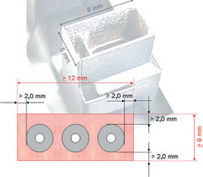
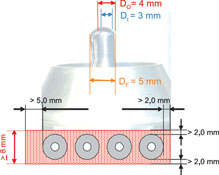
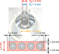
To perform a reliable soldering process, the minimum allowed inner diameter of a single miniwave soldering nozzle is 3 mm, which corresponds to an outer diameter of 4 mm. Minimum external dimensions for a soldering nozzle in multinozzle dip soldering processes are 5 x 8 mm.
To avoid difficulties caused by edge clearance, multinozzle dip soldering processes require a distance of at least 2 mm between the edges of the joints to be soldered to surrounding components or joints which should not be soldered. With a minimum nozzle size of 5 x 8 mm, this results in a clear area of 9 x 12 mm at least (Figure 3).
Depending on the specific process conditions, smaller clearances can be realised as well. This, however, needs to be checked thoroughly. It mainly depends on the type of neighbouring components and may require special measures, such as grippers with centring pins or the use of wettable solder nozzles. For miniwave soldering processes, board designers should consider 2 mm on three sides around a pin or a pin row and 5 mm on the side where the component leaves the wave, to allow proper peel-off (Figure 4). If a clearance of 5 mm is not possible at all, leaving the wave at an angle or the use of wetted solder nozzles can be helpful (Figure 5).
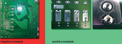
If board designers are not able to keep the required 2 mm distance on at least three sides, neighbouring SMD components should be aligned inline (Figure 6). The advantage of an inline alignment is that if the neighbouring, reflow soldered component is wetted during the selective soldering process, it will not immediately be washed away.

Single miniwave soldering in a drag process additionally requires consideration of the distance between the solder joint and a neighbouring component higher than 10 mm on the soldering side. When soldering with an angle, components higher than 10 mm could touch the soldering nozzle or gassing hood. As a rule of thumb for these specific components, the height of the component should be equal to or less than the distance to the solder joint.
Improved hole fill
The phenomenon of poor hole fill is mostly based on an insufficient heat transfer rate, which can also be improved with an appropriate PCB layout. The length of the component leads plays an important role in this regard, particularly in multinozzle dip soldering processes, which require a lead length greater than 2,5 mm. This is related to the energy transfer rate which directly affects hole penetration. Longer component leads are dipped deeper into the liquid solder, which improves the heat transfer and finally results in improved hole fill.
Another issue which should be considered in respect to hole fill is the ideal ratio between the pin diameter and the via. If this ratio should be too large, no capillary action will emerge. Should this ratio be too small, flux cannot soar through the via and therefore solder joints cannot be formed properly. As a rule of thumb, the diameter of the via should be equal to the diameter of the pin plus 0,2 to 0,4 mm. Lead-free processes can even require up to 0,5 mm.
Thermal energy will also be transferred better when the pad size is enlarged to a certain extent, or if oval pads are used. If possible, solder resist close to the solder joint should be avoided. This helps to keep the heat at the solder pad and also helps to avoid solder balling. Attention should also be given to thermal decoupling. With appropriate thermal decoupling of the PCB, the heat will not be completely withdrawn to the strip conductor, but will be held for a longer time at the pad (Figure 7).
Flowing solder waves, also in dip soldering processes, should generally be preferred. This ensures that oxide-free and correctly heated solder alloy is continuously supplied to the solder joints. Even during the contact phase, the solder alloy does not cool down. This improves hole fill remarkably, even in case of high-mass pins, at pins with connection to inner layers or pins which are located at the outer edges of an assembly.
Reduced solder bridging
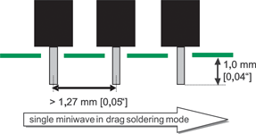
Solder bridges are a major reason for defects in selective soldering processes and are mainly caused by small distances between the component leads. Whereas multinozzle dip soldering processes require a pitch greater than 2,54 mm, single miniwave soldering processes allow smaller pitches of 1,27 mm. This applies for machine systems that facilitate setting of a soldering angle, which has an impact on the solder’s peel strength to reduce the risk of bridging, or for systems featuring wettable soldering nozzles.
Although pin rows with a lead distance smaller than 2,54 mm bear an increased risk of solder bridging in a dip soldering process, they can still be processed if some basic layout rules are considered. A smaller pad diameter, for example, can be helpful or, if possible, an oval pad form which helps to spread the liquid solder into a different direction, off the component leads. With specific modifications at the multi-nozzle soldering tool, a pitch to 2,0 mm can be realised as well.
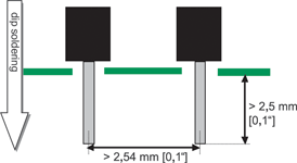
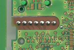
The length of the component leads plays an important role in regard to solder bridging as well. Multi-nozzle dip soldering processes require a lead length greater than 2,5 mm (Figure 8). The peel strength of the solder is enhanced with longer component leads, which pulls the solder away from the solder joint to reduce the risk of bridging.
In single miniwave soldering processes, the board is moved and usually a soldering angle is used to improve the solder’s peel-off. The typical lead length here should be around 1 mm (Figure 9). Shorter pins could cause poor meniscus formation and ball-shaped solder joints.
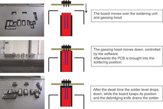
Particularly in the dip soldering process, an appropriate soldering nozzle design can significantly reduce the risk of solder bridging as well. So-called debridging knives, for example, in other words wettable plates which are installed inside the solder nozzle, drain the liquid solder after dwell time (Figure 10). Debridging knives are suited for special applications where the design rules mentioned earlier could not be followed, in other words where the pin length is smaller than 2,5 mm and/or pitch is between 2,54 mm and 2,0 mm.
Minimum solder balling
Solder balling is a phenomenon in all wave soldering processes – it has occurred in the past and it will occur in future. It appears more frequently, however, in lead-free soldering processes as process temperatures are significantly higher than in traditional soldering processes. The higher process temperatures can have a negative effect on the solder resist. Depending on the quality, the solder resist might soften during preheating, which results in solder balls sticking at the solder resist. In traditional lead bearing processes or applications featuring high-quality lead-free solder resists, developing solder balls would just bounce off. Therefore, if possible, solder resist close to the solder joint should be avoided (Figure 11).
Particularly in multinozzle dip soldering processes, special nozzle designs can help to avoid solder balling as well. These nozzle tools feature a defined solder flow which is directed by means of a flow plate. In addition, the complete nozzle tool is covered with a second top plate. Any splashes which might occur while the liquid solder is flowing back to the reservoir will therefore not get a chance to touch the printed circuit board.
Conclusion
Among all automated soldering processes, selective soldering is probably the most demanding process, requiring some experience and basic knowledge about the process itself and involved materials. Up-to-date selective soldering systems, however, already take care of most of the difficulties which could arise during the process.
By considering some basic board design rules, time-consuming and cost intensive repair soldering can be a thing of the past, while simultaneously increasing quality level of the manufactured products.


© Technews Publishing (Pty) Ltd | All Rights Reserved
 printer friendly version