28 October 2009Manufacturing / Production Technology, Hardware & Services
This article was originally published in Global SMT & Packaging magazine in April 2008, Vol 8, No. 4. Authors: Etienne Witte, Axiom Electronics and Paul Austen, ECD
Thermal profiling is a critical function in printed circuit board assembly. This article describes thermal profiling hardware and process management software solutions as used at American EMS provider Axiom Electronics to meet the thermal profiling challenges of today’s microelectronics environment. Reflow challenges include thermal inequalities of high layer-count circuit boards that have uneven mass distribution, components of varying sizes, micro BGAs, high ball-count BGAs, LGAs, etc. These easy to use thermal profiling tools help to improve yields by providing a stable, repeatable process while saving time and providing necessary supporting documentation.
Today’s challenges in thermal profiling
Although the electronics industry is often regarded as mature, new challenges continually occur. Some of these challenges, such as smaller parts and lead-free assemblies, require further development or modification of equipment, or changes in the control software. Component packages are available in more sizes, from 01005s to 50 mm² BGAs, and are being used side-by-side on the same circuit board. This can lead to problems when assemblies are thermally profiled for reflow. Layout, component size, package styles and thermal mass of the selected devices add to the challenge.
Thermal issues include different tolerated maximum temperatures, thermally sensitive components and different formulations of solder and flux. Lead-free assemblies compound the issues. Higher temperature requirements for lead-free reflow make it harder to avoid damage to sensitive components. To complicate matters, board assemblers may also encounter issues with hybrid boards that have a mix of lead-containing and lead-free components.
Reflow profiles that do not take all the above into account result in settings that produce unacceptable solder joints, failed components and overall low reliability.
Enter thermal profiling, the process of mapping the thermal effects that a reflow process has on the solder, components and PCBs that make up an assembly. The tool that has driven advances in thermal profiling is ECD’s M.O.L.E. thermal profiler, which in essence is the eye of the engineer inside the reflow oven. Initially, the capabilities of thermal profilers were limited to measuring minimum and maximum slopes and temperatures found in the oven and on the PCB. Engineers attached thermocouples to the bare PCB and beneath components to determine the delta-T (DT) between the different locations. This allowed the engineers to minimise thermal exposure to the most heat-sensitive parts while ensuring a proper reflow of the higher mass components.
The software for these initial devices provided simple ‘time versus temperature’ graphs, not data that was fully representative of the thermal process. Engineers still had to figure out how to modify the oven settings to achieve the required temperature profile and did so by using ‘tribal knowledge,’ experience and intuition. The added time in the production cycle reduced availability of the reflow oven for production during the trial and error phase and provided limited documentation of the process. Early profiling devices were bulky, poorly insulated, limited in the number of thermocouple channels and often unreliable. The components used in these profilers would often overheat, leading to inaccurate readings, lengthy cool-downs and even device failure. As components, solder formulations and PCBs evolved, new acquisition hardware, as well as new feature-rich analytical software, was needed.
Meeting the challenges
Axiom Electronics, a full-service EMS provider located in Beaverton, Oregon in the USA, deals with thermal challenges every day. Today’s SMT assemblies may contain mixed technologies/materials that produce a significant thermal gradient across the assembly in the x, y and z axes. Plated finishes for components and the PCB pads may be dissimilar, leading to solder joints that are unreliable. The PCB pads may not be optimally spaced to match the footprint of the component, which can lead to shifting or tombstoning of components. Different sized BGAs can tilt the profile toward high-mass, large BGAs, causing ‘voiding’ issues with smaller BGA packages during reflow.
If the solder goes to liquidus before all the volatiles evaporate, voids can form inside the solder balls (in extreme cases a ‘blowout’ on the ball could occur). BGA rework, an elaborate and time-consuming task involving specialty equipment and which should be avoided at all cost, is the unfortunate by-product. A thermal profiler may not solve all these problems, but it can quickly help engineers formulate and evaluate an oven recipe and resultant profile, yielding a process that works. For high reliability applications it is critical that there is a documented and repeatable reflow process. Using a unique reflow recipe for each product is the only way to ensure quality and long-term reliability.
Establishing the initial thermal profile
Modern software creates an initial thermal profile by analysing data provided by the engineer, such as board thickness, solder type, component size and thermocouple location. Full-featured software allows the engineer to include a component’s maximum temperature, ramp rate and solder paste being used (different solder pastes require different thermal profiles for optimum performance). Oven temperature settings and limits on conveyor speed are other variables that may be included.
Thermocouples are attached to parts located in areas of presumed thermal extremes on the assembly, and the PCBA is then run through the oven using the initial recipe provided by the profiling software. Once the oven run has been completed, the engineer uploads the data to the PC and the software makes an intelligent prediction. The engineer is then free to make adjustments to the prediction based on factors the software may not be aware of (eg, a lead-free BGA on an assembly processed with lead-free solder paste). The assembly is profiled again for process verification and documentation, with additional changes being made to the recipe as necessary.
Software is critical
Advanced software gives engineers the ability to review the suggested profile changes and fine-tune it as they see fit. It provides the ability to either use the recommended settings or modify the thermal profile based on the specific capabilities of their particular oven and production process. The ability to successfully predict and generate a custom recipe for each product is critical.
Engineers can enter the suggested settings (Figures 1 and 2), and the software will show changes in an overall prediction of what the profile will be, signalling changes that could compromise the required profile.
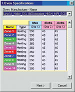
Figure 1. Software offers a large database of ovens and solder pastes to select
Auto-predictive features in the software then recalculate the values, and suggest oven settings that will achieve the required profile. The final thermal profile is an integrated part of the profiling software, which balances the needs of the thermal requirements of the solder paste, the limits of the assembly, the capabilities of the oven and the engineer’s knowledge of the SMT processes being used. Such tools allow Axiom to smoothly transition from general industry guidelines to settings refined for the more complex specialty PCBAs.
General industry guidelines</b>
General guidelines for ‘ramp-to-spike’ thermal profiles: 1°C/second ramp to a peak temperature of 20-30°C above liquidus for 30–60 seconds. Leaded SnPb 63/37 paste reflows at 183°C, lead-free SAC 305 at 217°C. Compromises and exceptions to these general guidelines are on an individual assembly basis. These values, as well as the values specified by the solder paste manufacturer, are used during thermal profiling.
The more capable the software, the more accurate the recipe provided, resulting in fewer lost assemblies or ruined ‘golden’ boards and prototypes. In addition, with intelligent software incorporating predictive algorithms, less time is required by engineers to profile. It is estimated that by simply freeing the engineers from additional profiling and other ‘OK to go’ authorisation tasks, this software could give board assemblers as much as one to two hours of extra production time per assembly that otherwise would have been used for profiling.
Temperature settings
The temperatures in the example are typical of a ramp-to-spike profile. If a ramp-soak-spike profile is desired (perhaps for a large BGA or a backplane PCB that needs time to come up to the desired temperature) the following temperature profile would be typical:
* Leaded process:
Ramp up from ambient temperature to 120°C at 1–2°C/second.
Soak at 120–160°C for 1–2 minutes.
Ramp up at 1–2°C/second from 140°C to peak temperature of 210–225°C.
* Lead-free process:
Ramp up from ambient temperature to 140°C at 1–2°C/second.
Soak at 140–200°C for 1–2 minutes.
Ramp up at 1–2°C/second from 170°C to peak temperature of 230–250°C.
Additional challenges: BGAs and lead-free
Assemblers face special thermal profiling challenges with BGAs, including concerns with voids or blowouts, mentioned earlier, which can form if the solder goes to liquidus too soon. PCBs may have multiple BGAs of different sizes on both the bottom and the top of the board. A profiler with a large number of thermocouples is beneficial since more than one BGA type or size will need to be profiled, and they will often be reflowed twice as a result of being on both sides of the board. Large BGAs may require more than one thermocouple to capture information from different locations under the BGA to determine if there is extreme thermal stress on the component. For PCBs with both large and small BGAs, assemblers have created special fixtures to shield heat-sensitive devices from the higher reflow temperatures required by larger BGAs, in the same way that fixtures are used in wave soldering processes. The goal is to ensure that all components receive only the heat they need to reflow properly.
Figure 3 shows a BGA that was removed from a customer assembly (left), cleaned (middle) and new solder spheres attached (right). This type of rework is performed on damaged boards and damaged BGAs, as well as for exchanging the type of spheres on a BGA (ie, removing lead-free spheres and installing leaded spheres). The MOLE is used to generate a profile that has a peak temperature of 195°C for leaded spheres and 227°C for lead-free spheres. Above that temperature, the spheres start to become wrinkled; if the process is hotter, the flux residues begin to char; if it is cooler, the spheres will not be uniform, and the spheres will not be coplanar (because spheres in the centre do not collapse as much as the spheres closer to the edge). A BGA with non-coplanar spheres will not sit flat on the PCB and may cause opens.
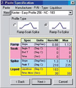
Figure 2. User-selectable assembly parameters
BGAs can pose other problems as well, and these problems occur at greater frequency with the increased use of lead-free solder. An example is two BGAs that became lead-free on a leaded assembly, but the customer continued to require leaded solder paste since all other parts were leaded. Engineers were able to use their knowledge of thermal profiles for lead-free components to make modifications to the existing profile. Since they knew that 210°C is the liquidus target for a leaded BGA and lead paste, the compromise was made that an additional 10 to 15°C should be added for the lead-free BGAs to ensure proper solder joints between the lead-free BGA balls and leaded solder paste. The engineer re-profiled this assembly using the new target temperature (225°C) and achieved successful reflow on the first board.
Electronics manufacturers have found survivability to be an issue for both leaded and lead-free components during lead-free processing. Some components that are labelled lead-free have no lead content but are not tolerant to a lead-free process window (ideally, a lead-free component should tolerate 250°C for a minimum of 30 seconds). Some lead-free components only permit a maximum temperature of 230°C for 10 seconds.
Since the solder manufacturer recommends 20°C above liquidus (217°C) for 30-60 seconds there can potentially be damage to the component. Terry Kern, senior manufacturing process engineer at Axiom, states, “When lead-free and leaded components are mixed on an assembly, the profile must be geared towards the survivability of the parts. This may not give every part its optimum processing, and finding the compromise that works best can be a challenge.” Software like ECD’s Xpert 3 allows the engineer to model ‘what-if’ scenarios to see which oven settings will produce the needed solder reflow profile for the solder while avoiding component damage, before they commit actual assemblies to the reflow oven process.
Other production benefits of thermal profiling
The prototype production lab at Axiom uses thermal profiling daily for applications such as BGA solder sphere reattach, solder pre-forms and BGA interposers. The thermal profiler can also be used to profile the curing of inks, adhesives, masks, etc. The profiles can help develop a process and result in quality improvement. A specific example of applying thermal profiling to an uncontrolled process follows.
A customer was using a heat gun (a very uncontrolled process) to reflow solder pre-forms. The pre-forms were being used to attach photodiodes to an assembly.
During the processing the customer experienced a diode fallout rate of 70%.
The use of a heat gun was damaging the diodes, either heating them too rapidly or exceeding maximum processing temperature. Rapid heating can cause a coefficient of thermal expansion (CTE) mismatch between the various materials inside the component, resulting in fractures within the component or the component packaging. It can also cause deterioration of organic materials within the component, resulting in either immediate failure or reduced service life.
When the project was brought to Axiom’s Lab, a thermal profiler was used to create a 1°C ramp rate to 20°C above the liquidus of the solder. This allowed the component to heat evenly, minimising CTE mismatch and keeping the maximum temperature within the component processing guidelines. The end result was a verified, repeatable reflow process that resulted in a 100% yield and eliminated the use of a heat gun.
According to Kern, “For contract and high-mix original equipment manufacturers, it is all about time.” In both environments, the engineer needs to complete an optimal thermal profile with no more than two trial runs. Profiling is not an exact science. Rather, it is a process that relies on the skills of the engineer to determine where to put the thermocouples, while using built-in knowledge from the software database about solder pastes and reflow ovens. This quickly and reliably creates an oven recipe, improves yields and saves time.
Axiom and other users find that extensive documentation provided by advanced profiling tools allows cross training of their engineering team, so that engineers may easily profile a PCB even if they are not familiar with its components. It also allows them to prove to their customers that the PCBs were soldered in accordance with the requirements of the SMT assembly and the solder paste, assuring reliable solder joints and higher yields.
Meeting the future challenges of thermal profiling
ECD, home of the M.O.L.E. profiler, has recently addressed issues such as status indicators by reducing the M.O.L.E.’s physical size to the thinnest in the industry and providing the following features:
* An ‘OK’ button that gives a clear Go/ No-Go signal.
* Rich data extractions, including delta-T.
* Improved documentation through customisable reports.
The ECD MAP software automatically measures the delta-T at peak from the profile and reports it in a table as well as indicating it on a profile graph. Other delta temperature parameters may be extracted, such as the maximum delta temperature between two temperatures, wherever it may occur, to measure the maximum stress on a component within a selectable temperature range. New software like ECD’s MAP sets a new standard in flexibility by offering over 180 unique measurement extractions.
The MAP software allows the user to customise the reports as well, providing the information their customers demand. A single page report may contain many elements to inform and confirm the SMT assemblies were soldered under the conditions demanded by the solder paste and tolerated by the assembly within the capabilities of the oven.
Thermal profiling systems typically have had only a few inputs as part of the thermal profiling package. However, a complex assembly with thousands of parts, many different sized BGAs and a mix of large, dense components and very small passive devices requires an engineer to use 15 or more different thermocouples to do thermal testing on and under components all over the assembly. In systems with only a few thermocouples, a PCB may need to run through the oven many times to develop all desired component profiles.
Any PCB has limits on the number of heat cycles it can survive without deterioration, so to avoid damage, engineers may use a solder sample board and dummy components. However, there are times when good boards must be used for profiling. Consequently, to limit possible damage to the PCB, engineers need systems with enough thermocouples to test as many components as necessary on the assembly in one oven pass. Thermal profilers such as the ECD MEGAM.O.L.E. 20 with twenty thermocouple inputs address this issue.
ECD has also addressed the MOLE size issue for nitrogen ovens. Nitrogen ovens have lower clearance and many of the current thermal profilers on the market are too thick to fit in these ovens. As a result, ECD designed the MegaM.O.L.E. 20, which is only 7,2 mm thick. Its protection barrier has been made thinner to fit most nitrogen ovens.
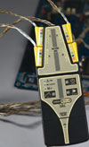
Figure 4. MEGAM.O.L.E. 20 and Nano 5-in-1 thermocouples
Thermal profiling has come a long way, from manually reading out temperatures from thermocouples and guessing what oven zone temperatures were required, to auto-predictive software that streamlines the profiling process and maximises standardisation and flexibility. ECD continues to work to lead the way in developing tools to meet these needs and set the standard for thermal profiling equipment.
200 W of power in a space-saving design Vepac Electronics
Manufacturing / Production Technology, Hardware & Services
The Hakko FX-972 Soldering Station delivers high-performance soldering in a compact package, making it suitable for a wide range of soldering applications.
Read more...FineX: Makes shielding clear Avnet Abacus
Manufacturing / Production Technology, Hardware & Services
Panasonic Industry launches high-transparency, low-resistance, flexible transparent conductive film for electromagnetic wave shield with pre-applied OCA.
Read more...Collaboration is now critical RS South Africa
Manufacturing / Production Technology, Hardware & Services
The message emerging from RS Connect is clear: Organisations can no longer rely on internal optimisation alone to secure performance. Competitive advantage is increasingly being determined by the strength of external relationships, shared capability and coordinated action across value chains.
Read more...Disruption is the new normal. Effortless is the new competitive advantage. Seven Labs Technology
Manufacturing / Production Technology, Hardware & Services
Global supply chains have been under pressure for years. The manufacturers still standing are the ones who stopped waiting for normal to return, and started building something better.
Read more...World-first 016008 mm component placement
Manufacturing / Production Technology, Hardware & Services
Fuji has achieved the world’s first placement of 016008 mm (0,16 x 0,08 mm or 006 x 003 inches) size components on printed circuit boards with its SMT pick and place machine, NXTR.
Read more...Lifecycle and obsolescence: Protecting electronics through process Production Logix
Manufacturing / Production Technology, Hardware & Services
At Production Logix, we believe longevity is not accidental. It is engineered through early visibility, structured response, and disciplined execution, in partnership with our OEM customers.
Read more...Maximising squeegee quality and durability Testerion
Manufacturing / Production Technology, Hardware & Services
Transition Automation has announced two new product advancements designed to improve SMT printing performance and extend squeegee life: laser-enhanced Permalex bonding and integrated edge protectors.
Read more...NeoDen ND2 PCB screen printer ZETECH ONE
Manufacturing / Production Technology, Hardware & Services
The NeoDen ND2 PCB screen printing machine is a fully automatic stencil printer designed to deliver precise and consistent solder paste application in modern SMT production environments.
Read more...Understanding the BGA rework process Techmet
Manufacturing / Production Technology, Hardware & Services
BGA rework is a highly technical process that involves removing the faulty component, preparing the circuit board, and installing a new or repaired device, while maintaining the integrity of the printed circuit board.
Read more...Flexible three-process reflow soldering system Truth Electronic Manufacturing
Manufacturing / Production Technology, Hardware & Services
By combining multiple soldering technologies within a single system, the Vision TripleX system enables manufacturers to adapt easily to different assembly requirements, board designs, and production volumes.
While every effort has been made to ensure the accuracy of the information contained herein, the publisher and its agents cannot be held responsible for any errors contained, or any loss incurred as a result. Articles published do not necessarily reflect the views of the publishers. The editor reserves the right to alter or cut copy. Articles submitted are deemed to have been cleared for publication. Advertisements and company contact details are published as provided by the advertiser. Technews Publishing (Pty) Ltd cannot be held responsible for the accuracy or veracity of supplied material.


 printer friendly version