


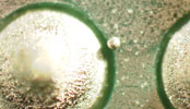
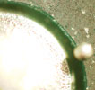
There are two types of solder balls generally seen after wave soldering; they can be referred to as consistent/repeating or random balls. Obviously there are lots of theories on how they form and bond to the surface of the solder mask. The following figures are taken from Bob Willis archives and show the many sides of ball formation.
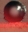
Random solder balls
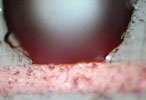
The balls vary in size and are positioned randomly on the base of the board. Some evidence of solder balls can also occur on the top surface of the board after wave or selective soldering. Basically the solder balls have either formed due to spitting or outgassing due to the flux volatile not being dried prior to wave solder contact. The solder literally explodes on the surface of the wave and the solder particles then bond to the soft surface of the solder mask or remaining flux.
Seeing balls on the top side of the board generally indicates an increased severity of the problem. They normally blow through tooling hole cutouts on the surface of the board. If the copper plating in the hole is poor, solder balls can be ejected out of plated through-holes as the water vapour in the board expands; in this case flux is not the root cause. When there is a lot of evidence of random solder balls from wave contact, surfaces around the wave ducting will be covered in small balls. There will also be evidence of the balling on the inside top surface of the hood over the wave and all over the pallets.
If the wave is being pumped higher than 5–6 mm to accommodate other parts of the process, the solder returning to the solder bath can produce solder balls. This can be seen on an air system directly after de-drossing the solder surface and less so after the solder starts to form an oxide layer. The oxide on the wave suppresses the solder from bouncing back from the surface. This is seen more commonly on a nitrogen wave.
The use of an air knife after the wave can generate solder balls on the top side of the board with excess air or nitrogen pressure or incorrect angle of the knife to the board. This normally occurs when engineers are trying to increase the performance of the knife and blow solder out of through-holes. It is particularly difficult if a wide range of plated through-holes sizes, non-plated through-holes or cutouts are present on one board design.
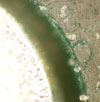
Consistent/repeating balls
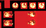
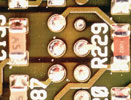
Solder balls are often seen in a no-clean process positioned between terminations on SOIC, QFP and SOT terminations or on through-hole components like integrated circuits, IDC post headers or sockets. The ball is positioned between adjacent pins as the solder separates; the solder web between two pins does not always separate in the middle, so the ball is not always in the centre of the pins. On wave soldering the solder ball tends to drain from back to front, while on multirow connectors like IDC headers the solder can drain to the side at 45°, leaving the ball in a different location on the mask. This is more noticeable on selective solder nozzles where the width of the solder jet is often equal to the group of pins.
Normally, close examination shows the solder balls bonded to the solder mask with a thin flux layer around the base. This is not normally seen in nitrogen or on random balls. Careful mechanical removal of the ball often shows some surface bond was present, indicating a softening/attack of the mask surface, as illustrated by the samples in Figure 3.
A combination of flux and solder mask are the most often used parameters to reduce and eliminate consistent/repeating balls with the mask being the major factor. Side by side trials have shown that a rougher surface is better to reduce solder ball adhesion, however there are many contradictory parameters.
In the early days of no-clean, one option was to use a rotary brush to remove the balls from the base of the board directly after wave soldering. Some wave solder suppliers still offer brush modules as part of an outfeed conveyor system.
IPC 610D – Acceptability of electronic assemblies
The following is the current text in IPC 610D which relates to solder balling or solder splashing. For this criteria to be applied and used in a manufacturing environment the quality department must confirm this minimum design clearance specification.
5.2.6.1 Soldering anomalies – excess solder – solder balls/solder fines
Solder balls are spheres of solder that remain after the soldering process. Solder fines are typically small balls of the original solder paste metal screen size that have splattered around the connection during the reflow process.
Target – Class 1,2,3: No evidence of solder balls on the printed wiring assembly.
Acceptable – Class 1,2,3: Solder balls are entrapped/encapsulated and do not violate minimum electrical clearance.
Note: Entrapped/encapsulated/attached is intended to mean that normal service environment of the product will not cause a solder ball to become dislodged.
Defect – Class 1,2,3: Solder balls violate minimum electrical clearance
Solder balls are not entrapped in no-clean residue or encapsulated with conformal coating, or not attached (soldered) to a metal surface.
IPC 610 – Acceptability of electronic assemblies
The following was the solder balling/splatter criteria for previous/older versions of the IPC standard and referred to in other telecommunication standards and customer defined standards:
Solder balls are spheres of solder that remain after the soldering process. Solder fines are typically small balls of the original solder paste metal screen size that have splattered around the connection during the reflow process.
Acceptable – Class 1/Process indicator – Class 2,3: Entrapped or encapsulated solder balls that are within 0,13 mm of lands or conductors, or exceed 0,13 mm in diameter. More than five solder balls/splashes 0,13 mm or less per 600 mm².
Defect – Class 1,2,3: Solder balls violate minimum electrical clearance. Solder balls not entrapped or encapsulated (eg, no-clean residues, conformal coating), or not attached to a metal surface.
Note: Entrapped/encapsulated/attached is intended to mean normal service environment of the product will not cause a solder ball to become dislodged.
For more information visit www.askbobwillis.com


© Technews Publishing (Pty) Ltd | All Rights Reserved
 printer friendly version