


This article provides some handy rules of thumb for those designing and assembling printed circuit boards with package on package devices.
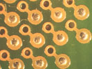
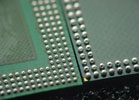
Copper pad size
The copper pad size used on the printed board surface will be dependent on factors such as the ball size of the package being assembled, experience of other packages with similar terminations, placement accuracy etc. Typically engineers will often use the same termination pad size used on the component body. Too large a pad size takes up valuable design space and also reduces package stand-off height for a given paste ball volume. This is due to the solder wetting out to the edge of the pad which also defines the stand-off height.
As a typical example, for a ball size of 0,3 mm, the copper pad size of a copper defined pad will be approximately 0,22 mm. In the case of a resist or solder mask defined pad, the mask opening would be 0,22 mm and the copper pad larger to increase surface adhesion.
Via in pad
As with ball grid arrays (BGAs) the tracking can fan out from the pad to a lower layer of the board stack using a via hole of 0,2-0,4 mm. However, with PoP devices commonly on a 0,4-0,5 mm pitch, this is not really as feasible, hence the need to use via in pad or stacked via interconnection.
As an example, a blind via hole may be 0,1 mm. It is recommended that any via in pad design for PoP has the via filled or plated up during PCB manufacture to eliminate void formation during paste reflow.
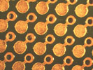
Solder mask options
There are two options in design for PoP: either solder mask or copper defined pads. The most conventional design practice is copper defined pads.
Copper defined pads are just regular pads with a solder mask clearance of between 0,05 and 0,076 mm around the copper pad, which is based on the PCB supplier’s capability and a combination of the laminate and solder mask system being specified.

Solder mask defined pads are where the design engineer uses larger pads on the surface of the board but creates a solder mask aperture that is smaller than the pad. The solder mask is then overlapping the copper pad; hence the mask defines the pad size. Obviously the stand-off of the package is still defined by how far the solder paste and ball can wet out as they both coalesce together. It is also easier to produce a wetting indicator in the resist layer.
As an example, a design engineer may use a copper pad size of 0,4 mm and a solder mask opening of 0,22 mm and end up with a solder mask hanging over the copper to better anchor the copper pad to the substrate.
The thickness of the solder mask on a board should be defined like any other surface mount application. In addition, the compatibility of the mask and the underfill (if used) needs to be reviewed. The adhesion of the underfill to the mask is a key factor to reliability; this is also the case if corner bumping is going to be used.
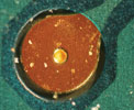
Corner alignment marks
Positioned at the outer corners of each PoP device are inspection/alignment marks in the form of a chevron. The marks are positioned and aligned with the edge of the component body, allowing any misplacement of the device to be assessed visually. The marks are etched into the copper on the surface of the board so that accurate alignment can be monitored with the pad artwork.

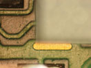
This form of mark needs to be included on any board to aid inspection for misplacement, alignment during hand placement or during rework. It is perfectly acceptable to just have two marks on opposite corners of a device etched in to the copper but not to use legend ink which is in most cases not feasible with PoP designs.
Although these marks date back to the early introduction of BGA technology, they are still used today and often seen with PoP on mobile phone applications. Sometimes chevrons are not used, but rather a short copper line on two opposite corners is featured on mobile design application. As an example, the dimensions of the chevrons are 0,16 mm wide and 0,4 mm long. Creating apertures in the solder mask is another technique that can be used for alignment and inspection.
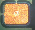
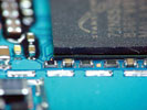
Inspection wetting indicators
Wetting indicators on pads allow the solder to reflow in a selected area of the pad and change the actual shape of only selected joints. These may be positioned at the four corners of a design and possibly in four positions in the centre area of larger devices. The aim of this design trick is to make inspection using X-ray easier. It is not the only solution but it is beneficial and costs nothing, even if never used as an aid.
Component clearances
Ideally there should be a clearance around the component body outline to allow for rework, underfill and optical inspection using an endoscope inspection system. As a basic guide, the clearance would be a minimum of 2 mm but you will need to consider the equipment used in manufacture as systems vary – some inspection angled mirrors require 4 mm clearance.
Depending on the equipment, this is also a vertical height requirement, not just on the surface of the board. It may not be possible to have a clearance around the complete edge of a PoP stack as passive components are required for decoupling. Try and leave the corners of the device free and mount the passive parts in the centre of each edge of the device or leave a minimum of two adjacent sides free.

PoP bill of materials
Care needs to be taken during a design review over the bill of materials (BOM); this is particularly true in a subcontract environment when sales staff and purchasing are the first to review a BOM for costing and possible procurement of parts. PoP devices may be listed as one or multiple parts so the requirement for PoP assembly may not be obvious at the assembly quoting stage.
It is common to find that each of the devices that make up a PoP structure is listed as separate items with their own supplier part numbers. Having just one reference number may only be the case if the part has already been assembled as a preassembled PoP device by a specialist packaging house. Another point which can be confusing when examining a BOM, but also suggests a stacked package, is when a single component reference designator is used for two or three parts.
All dimensions mentioned in this article are provided as a reference only. Engineers should check with component suppliers and PCB manufacturers for their own process capability.
The author has created a complete training resource for package on package design, assembly and process control, with online training sessions with Electronics Production World, hands-on training sessions, interactive CDs and inspection posters all available at www.packageonpackage.co.uk
For more information visit www.askbobwillis.com


© Technews Publishing (Pty) Ltd | All Rights Reserved
 printer friendly version