Manufacturing / Production Technology, Hardware & Services


ESD floor coverings

22 February 2012 Manufacturing / Production Technology, Hardware & Services

Many people do not know the difference between static dissipative and static conductive flooring.

In order to understand what makes these two floor coverings different, one needs to first understand what they are designed to do, and why.

The human body can generate up to 30 000 Volts in static electricity depending on the type of clothing we wear, the type of upholstery we sit on or floor coverings we walk on. The resulting discharge from the electron imbalance when we touch a grounding source is often felt as a static shock when touching another object. This energy discharge is problematic when working with flammable gasses or sensitive electronic equipment, and the static charge needs to be dissipated via ESD floor coverings or other ESD products, in a controlled manner in order to avoid damage to equipment or people.

ESD flooring is an excellent form of facilitating a uniform flow of static electricity directly to a ground point. Most types of vinyl flooring claim to be anti-static. This means that they do not contribute towards the build-up of static electricity in the human body. They also do not drain the static charge already built up. High levels of static are generated in dry areas, and conditions are much worse inland away from the coast.

The international norm for an electrically conductive floor covering is that it should have a resistance to earth level of between 104 and 106 Ω and an electrically dissipative floor should be between 106 and 109 Ω. It stands to reason that the electrically conductive floor covering will drain the static charge more quickly than an electrically dissipative floor covering as it has lower resistance to earth.

So what is the difference?

Static dissipative (SD) floor coverings are chemically treated to discharge static electricity and must be used in a controlled environment with a relative humidity of above 40%. Typical areas of use would be operating theatres, computer areas and instrument control rooms.

Electrostatic conductive (EC) floor coverings contain carbon and discharge static electricity more quickly and can be used in less controlled environments. In controlled environments they would be used in sensitive electrical and assembly areas as well as explosive manufacturing areas.

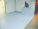
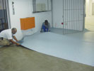
Electrostatic conductive and dissipative floor coverings are usually laid on a cement subfloor. Concrete is a poor conductor of electricity, so this type of floor covering needs to be laid using a conductive adhesive and earthed in order to drain the discharge. Aluminium or copper tape is laid in the adhesive under the floor covering and taken to an earth point. Two earth points are used in case one fails. For larger areas one earth point is allowed for every 20 m².

The floor coverings are available in both sheet and tile form. The tile sizes are 608 x 608 mm in order to accommodate raised access floors. Raised access floors are usually made of steel, to ensure that the legs are earthed. As a rule, electrostatic dissipative floor coverings are never sealed, as this would create a barrier between the floor covering and the human body and so prevent discharge. Conductive sealers are available if required.

Actum Electronics offers a comprehensive range of static control solutions and can be enlisted in order to do an audit of premises prior to specification, installation, testing and certification. The company has partnered with flooring experts Polyflor for all ESD flooring requirements. ESD flooring clients include Vodacom, Nissan, Grintek Ewation, Nokia, Armscor, MTN, Motorola, SAAB Technology, Denel and Mecer, amongst others.


Credit(s)


Share this article:
Share via emailShare via LinkedInPrint this page

Further reading:

Clearing the Static: ESD containers and packaging
Actum Circuit & System Protection
         Vacuum forming ESD Electronic components can be damaged by electrostatic discharges. To protect against such damage, electronic assembly parts are often transported or stored in vacuum formed component ...

Read more...
Outscale your competition
Manufacturing / Production Technology, Hardware & Services
Attendees will be able to explore the benefits of AMD Kintex UltraScale+ Gen 2 FPGAs in high-performance Pro AV, test & measurement, industrial, and medical applications.

Read more...
MTN SA Foundation drives youth pathways into the digital economy
Manufacturing / Production Technology, Hardware & Services
The MTN SA Foundation, in partnership with Helios Towers and Datacomb Development Hub, has launched the MTN–Helios Towers 12-month ICT Learnership Programme, a pathway that takes young South Africans from digital training into real workplace experience.

Read more...
Downstream demand, system reliability, and the expanding role of engineering-led distribution
Manufacturing / Production Technology, Hardware & Services
[Sponsored] As South Africa’s semiconductor demand continues to be shaped by downstream system deployment rather than upstream fabrication, the importance of engineering-led distribution will continue to grow.

Read more...
The impact of harsh environments and ionic contamination on post-reflow circuit assemblies
MyKay Tronics Manufacturing / Production Technology, Hardware & Services
There is well documented historical proof that post-reflow circuit assemblies, when subjected to harsh environments, are particularly vulnerable to failure mechanisms, but modern electronic assemblies are far more susceptible to this phenomenon.

Read more...
Engineering copper grain structure for high-yield hybrid bonding in 3D packaging
Testerion Editor's Choice Manufacturing / Production Technology, Hardware & Services
The way copper grains are sized and distributed forms the metallurgical foundation of hybrid bonding, enabling lower bonding temperatures, greater reliability, and stable grain structures throughout integration.

Read more...
Understanding solder dross: causes and control strategies
Truth Electronic Manufacturing Editor's Choice Manufacturing / Production Technology, Hardware & Services
Dross formation is an inevitable consequence of wave soldering. It occurs when molten solder comes into contact with oxygen, forming metal oxides that float on the surface of the solder bath. Over time, this oxidation byproduct accumulates and must be removed to maintain solder quality and process consistency.

Read more...
Non-destructive techniques for identifying defects in BGA joints – TDR, 2DX, and cross-section-SEM comparison
MyKay Tronics Manufacturing / Production Technology, Hardware & Services
This whitepaper reports the results of a comparison of the following techniques: TDR, automatic X-ray inspection (AXI), transmission X-ray (2DX), cross-section/SEM, and Dye & Pry.

Read more...
Implications of using Pb-free solders on X-ray inspection of flip chips and BGAs
MyKay Tronics Manufacturing / Production Technology, Hardware & Services
With the move to Pb-free soldering, most of the attention has been paid to reflow temperatures, component compatibility, and reliability concerns, but the implications for inspection, particularly X-ray inspection, are equally important and often underestimated.

Read more...
The causes of solder balls in robotic soldering
Manufacturing / Production Technology, Hardware & Services
Solder balls (also known as solder splatter) are a major concern in many production sites as they may potentially cause shorts, leading to long-term impacts on product reliability.

Read more...


While every effort has been made to ensure the accuracy of the information contained herein, the publisher and its agents cannot be held responsible for any errors contained, or any loss incurred as a result. Articles published do not necessarily reflect the views of the publishers. The editor reserves the right to alter or cut copy. Articles submitted are deemed to have been cleared for publication. Advertisements and company contact details are published as provided by the advertiser. Technews Publishing (Pty) Ltd cannot be held responsible for the accuracy or veracity of supplied material.


© Technews Publishing (Pty) Ltd | All Rights Reserved