


This article identifies the key parametric considerations for comparing IGBT and MOSFET performance in specific SMPS (switch mode power supply) applications. Parameters such as switching losses are investigated in both hard-switched and soft-switched ZVS (zero voltage switching) topologies.
The three main power switch losses – turn-on, conduction and turn-off – are described relative to both circuit and device characteristics.
The impact of diode recovery performance on hard-switched topologies is also discussed, illustrating that diode recovery is the dominant factor determining MOSFET or IGBT turn-on switching losses.
This article also shows how device selection is complicated by the specific cooling system being utilised. For example, a single IGBT may perform well in a hard-switched PFC (power factor correction) circuit with sufficient cooling heatsink; while, conversely, a design that mandates a marginal heatsink for cost or space reasons may require multiple parallel power MOSFETs.
The conclusion reiterates that there is no single solution for choosing and applying IGBTs or MOSFETs in SMPSs and that each application merits careful analysis in selecting an optimum switching device.
Historically, the off-line SMPS industry has been driven by the power semiconductor industry’s power component advancements. As the main power-switching devices – IGBTs, power MOSFETs and power diodes – continually improve, there are corresponding and significant efficiency, size, weight and cost improvements in SMPS designs.
Because of this direct component-to-application performance relationship, SMPS designers must compare the many pros and cons of the various semiconductor technologies to optimise their designs. For example, MOSFETs typically excel for lower-power and higher-frequency applications, i.e., power levels < 1000 W and switching frequencies ≥ 100 kHz. But IGBTs have distinct advantages for lower-frequency and higher-power designs.
This article compares an IGBT, the FGP20N6S2D SMPS2, and a MOSFET, the FCP11N60 SuperFET (from Fairchild Semiconductor) in an SMPS application. These products exemplify state-of-the-industry parts and they have comparable die size and identical thermal resistance RJC.
Turn-on losses
The turn-on characteristics of IGBTs and power MOSFETs are quite similar, except that IGBTs have a longer voltage fall time. Referencing the basic IGBT equivalent circuit (Figure 1) the time required to fully modulate the minority carrier PNP BJT collector base region results in a turn-on voltage tail. This delay results in a quasi-saturation effect wherein the collector-emitter voltage does not immediately fall to its VCE(sat) value1.
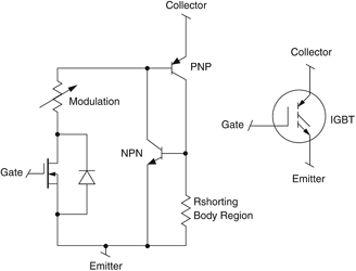
This turn-on effect also results in a VCE voltage bump under ZVS conditions at the point where the load current transitions from the co-packed inverse parallel diode to the IGBT collector. The Eon energy losses specified in datasheets is the time integral of Icollector times VCE in joules per switching cycle, and includes the additional losses associated with quasi-saturation.
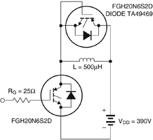
Two Eon energy parameters, Eon1 and Eon2, are provided in IGBT datasheets. Eon1 is the energy loss without the losses associated with hard-switched diode recovery. Eon2 includes the hard-switched turn-on energy loss due to diode recovery and is measured by recovering a diode identical to the co-packed diode associated with the device.
A typical Eon2 test circuit is illustrated in Figure 2. The test is performed with the diode at the same Tj as the device under test. The IGBT is switched through two pulses to measure Eon. The first pulse raises the inductor to the desired test current and the second pulse then measures the Eon loss recovering this current from the diode.
Under hard-switched turn-on, the gate drive voltage and impedance and the recovery characteristics of the commutated diode determine the Eon switching loss. For circuits such as the conventional CCM (continuous current mode) boost PFC circuit, the boost diode recovery characteristics are extremely important in controlling Eon (turn-on) energy losses.
In addition to selecting a boost diode with minimal Trr and QRR, it is also important to ensure that the diode has soft recovery characteristics. Softness, the ratio of tb/ta, has a considerable impact on the electrical noise and voltage spikes generated across the switching device. Snappy diodes with a rapid tb period di/dt fall from IRM(REC) create large voltage spikes in the circuit parasitic inductances. These voltage spikes create EMI and can result in excessive reverse voltage across the recovering diode.
In hard-switched circuits, such as the full-bridge and half-bridge topologies where the IGBT co-packed diode or the MOSFET body diode is conducting when the alternate switching device is turned on, the diode recovery characteristics determine the Eon loss. For this reason it is important to select MOSFETs with fast body diode recovery characteristics.
Unfortunately, MOSFET parasitic, or body diodes, are relatively slow compared to state-of-the-industry discrete diodes. For hard-switched MOSFET applications, the body diode is often the limiting factor determining the SMPS operating frequency.
Typically, IGBT co-packed diodes are selected for compatibility with their intended applications. Slower ultrafast diodes with lower forward conduction losses are co-packed with slower lower-VCE(sat) motor drive IGBTs. Conversely, soft recovery hyper-fast diodes, such as the Fairchild Stealth series, are co-packed with the high-frequency SMPS2 switched mode rated IGBTs.
Beyond selecting the right diode, a designer can control Eon losses by adjusting the gate drive turn-on source resistance. Decreasing the drive source resistance will increase the IGBT or MOSFET turn-on di/dt and decrease the Eon loss.
The tradeoff is between Eon losses and EMI, since the higher di/dt will result in increased voltage spikes and radiated and conducted EMI. Selecting the correct gate drive resistance to meet a desired turn-on di/dt may require in-circuit testing and verification.
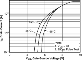
A ballpark value may be determined from the MOSFET transfer curve (Figure 3). Assuming the FET current will rise to 10 A at turn-on, and looking at the 25°1C curve of Figure 3, the gate voltage must transition from 5,2 V to 6,7 V to reach 10 A and the average GFS is 10 A/(6,7 V-5,2 V) = 6,7 mhos.
The gate drive resistance for a desired turn-on di/dt is calculated as:
Applying this average GFS value to Equation 1, with a gate drive of Vdrive = 10 V, a desired di/dt = 600 A/μs and typical FCP11N60 values VGS(avg) = 6 V, Ciss = 1200 pF; a 37 Ω turn-on gate drive resistance is calculated. Since the instantaneous GFS value is the slope in Figure 3, GFS will vary during the Eon period, which implies a varying di/dt.
The exponentially decaying gate drive current and decreasing Ciss as a function of VGS also enter into this equation with an overall effect of surprisingly linear current rise.
Similar gate drive turn-on resistance may be calculated for the IGBT. Again
VGE(avg) and GFS may be determined from the IGBT transfer characteristic curve, and the CIES value at VGE(avg) should be substituted for Ciss. The comparable calculated IGBT turn-on gate drive resistance is 100 Ω. This higher requirement is indicative of the higher IGBT GFS and lower CIES. A key point here is that gate drive circuit adjustments must be made for a transition from MOSFET to IGBT.
This article will be continued in the next issue of Dataweek.
| Tel: | +27 11 923 9600 |
| Email: | [email protected] |
| www: | www.altronarrow.com |
| Articles: | More information and articles about Altron Arrow |


© Technews Publishing (Pty) Ltd | All Rights Reserved
 printer friendly version