


The first part of this article was published in the 30 May issue of Dataweek.
Conduction losses
When comparing 600 V rated devices, IGBT conduction losses typically are less than an equivalent die size 600 V MOSFET. A qualifier is that the comparison should be made at appreciable collector and drain current densities and at the desired worst-case operating junction temperature.
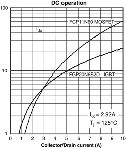
For example, the FGP20N6S2D SMPS2 IGBT and FCP11N60 SuperFET both have an RθJC value of 1°C/W. Figure 4 compares conduction loss versus DC current at a junction temperature of 125°C. It shows that the MOSFET will have more conduction losses for DC currents greater than 2,92 A d.c.
However, the DC conduction loss comparison in Figure 4 does not apply to most applications. In Figure 5, on the other hand, conduction losses are compared operating in a CCM, boost PFC circuit with a junction temperature of 125°C and V a.c. input of 85 V and 400 V d.c. output. In this figure the MOSFET-IGBT crossover point is 2,65 A RMS.
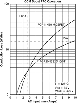
For PFC circuit, AC input currents greater than 2,65 A RMS, the MOSFET will have greater conduction losses. The 2,65 A PFC AC input current equates to 2,29 A RMS in the MOSFET as calculated by the following equation for boost switch RMS current in a CCM PFC circuit:
Where:
* IacRMS is the PFC circuit RMS input current
* Vac is the PFC circuit RMS input voltage
* Vout is the DC output voltage
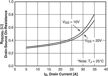
The MOSFET conduction loss is calculated as an I²R loss using the current defined by Equation 2 and the MOSFET 125°C RDS(on). This conduction loss may be further refined by accounting for the variation of RDS(on) as a function of drain current. This relationship is illustrated in Figure 6.
The impact on conduction losses may be determined as outlined in an IEEE article called ‘How to include the dependency of the RDS(on) of power MOSFETs on the instantaneous value of the drain current into the calculation of the conduction losses of high-frequency three-phase PWM inverters’2.
The impact of RDS(on) change as a function of ID is minimal for most SMPS topologies. As an example, the impact of operating the FCP11N60 MOSFET in the PFC circuit to an ID of 11 A peak current, or two times the 5,5 A, its RDS(on) is specified at will increase the effective RDS(on) and conduction losses by 5%.
The RDS(on) characteristic illustrated in Figure 6 should be considered in topologies where the MOSFET conducts high pulse currents for very short duty-factor. If the FCP11N60 MOSFET is operated in a circuit with a 20 A pulse at 7,5% duty-factor (i.e., 5,5 A RMS), the effective RDS(on) will be 25% greater than the specified 0,32 Ω at 5,5 A.
It is more complex to calculate the IGBT conduction loss in applications, such as a PFC circuit, where each switching period is at a different ICE.
This is because the VCE(sat) cannot be represented as a resistance voltage drop. A relatively straight-forward approach is to represent the IGBT VCE(sat) as a fixed VFCE voltage in series with a resistor RFCE. VCE (ICE) = ICE X RFCE + VFCE.
The conduction losses may then be calculated as the product of the average collector current times VFCE, plus the RMS collector current squared, times the resistance RFCE. This technique is detailed in the articles referenced below3,4, which include validation in a PFC circuit.
The loss curves in Figure 5 consider only the IGBT and MOSFET conduction losses in a CCM PFC circuit. If, as an example, the design objective is to maintain the worst-case conduction losses to less than 15 W, then using the FCP11N60 MOSFET, the circuit is limited to 5,8 A.
However, the FGP20N6S2D IGBT can operate with an AC input current of 9,8 A, which means it can handle 70% more power with this 15 W conduction loss restriction.
While IGBTs will exhibit lower conduction losses, most 600 V IGBTs are PT (punch-through) devices. PT devices have an NTC (negative temperature coefficient) and will not share current when operated in parallel. PT devices may be paralleled with limited success by matching device VCE(sat), VGE(TH) (gate-to-emitter threshold voltage), and by mechanically packaging such that the IGBT die temperatures will track closely.
Conversely, the MOSFET has a PTC (positive temperature coefficient) that provides good current sharing.
Turn-off losses
MOSFETs have considerably lower turn-off losses than IGBTs in hard-switched, clamped inductive operation. This is because of the IGBT tail current associated with clearing the minority carriers, which are associated with the PNP BJT (Figure 1).
IGBT Eoff energy curves as a function of collector current and junction temperature (Figure 7) are provided in most IGBT datasheets. These curves are applicable for a fixed clamped inductive test voltage and include the tail current energy loss. Figure 2 illustrates the typical test circuit used for measuring IGBT Eoff as a function of ICE and Tj.
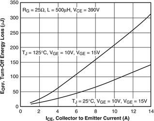
The Eoff test voltage, the VDD in Figure 2, varies with manufacturer and the specific device’s BVCES. This test VDD should be considered when comparing devices. Testing and operating at a lower VDD clamp voltage will result in reduced Eoff energy loss.
Lowering the gate drive turn-off resistance will have minimal effect in reducing IGBT Eoff loss. As illustrated in Figure 1, once the equivalent majority carrier MOSFET is turned off there is still a td(OFF)I storage time delay in the IGBT minority carrier BJT. Lowering the Eoff drive resistance will, however, reduce the risk of the Miller capacitance CRES and turn-off VCE dv/dt injecting a current into the gate drive that re-biases the device into conduction causing multiple Eoff switching.
ZVS and ZCS (zero current switching) topologies have advantage in reducing turn-off losses in both MOSFETs and IGBTs. The ZVS operation advantage is not as great in IGBTs since an Eoff tail bump current, albeit smaller, will still exist once the collector voltage rises to a potential that permits dissipation of excess stored charge.
ZCS topologies produce the greatest IGBT Eoff performance improvement. Proper gate drive sequence, wherein the IGBT gate signal is not removed until the point of second collector current zero crossing, can have a marked improvement in IGBT ZCS Eoff reduction5.
The MOSFET Eoff energy loss is a function of its Miller capacitance Crss, the gate drive speed, gate drive turn-off source impedance, and parasitic inductance in the source power circuit path. The circuit parasitic inductance Lx, shown in Figure 8, generates a potential that increases the turn-off loss by limiting the current fall di/dt.
At turn-off, the current falls at a di/dt determined by Lx and VGS(th). If, as an example, Lx = 5 nano-henries and VGS(th) = 4 V the maximum rate current fall will be VGS(th)/Lx = 800 A/μs.
Gate drive requirements
While both MOSFETs and IGBTs have high gate impedance and are voltage-controlled devices, the minimum-drive voltage requirements are different. The minimum acceptable gate drive voltage is important, since falling below this value will result in switching from the ‘on’ state to a highly dissipative linear mode.
Drive circuits for either device should be designed such that the gate drive does not fall below the minimum value under any condition. Good circuit design mandates that a gate drive UVLO (under-voltage lockout) circuit be incorporated to ensure that gate drive is removed for low drive voltage conditions to prevent the switching devices from entering linear conduction mode.
When comparing the FGP20N60S2D and FCP11N60 gate characteristics, the FGP20N60S2D’s VGEP plateau voltage is 8 V max and the FCP11N60 VGS(th) threshold voltage is 5 V max. The FGP20N60S2D IGBT VGEP value is meaningful since it is tested at an appreciable 7 A current. However, the FCP11N60 MOSFET VGS(th) voltage is measured at 250 μA and does not guarantee that the device will be ‘on’ at a VGS of 5 V.
Further useful information may be obtained from the MOSFET’s VGS versus ID on-region characteristic curve. For example, in order to guarantee that the FCP11N60 is ‘on’ for a 10 A load, the VGS should be 6,5 V minimum.
Parasitic gate capacitances heavily impact the switching characteristics of both MOSFETs and IGBTs. For the MOSFET the drain-to-gate Crss, reverse transfer capacitance, in conjunction with the gate drive source resistance, determines the rate of drain voltage fall at turn-on and rise at turn-off.
The IGBT collector-gate CRES capacitance acts similarly by limiting the rate of VCE fall at turn-on. At turn-off, the IGBT CRES may cause multiple switching if the gate drive resistance Roff is not sufficiently small. In this case, the equivalent MOSFET (Figure 1) turns off, but the VCE does not rise until after the excess charge is cleared from the BJT. At that point, the rapidly rising collector voltage and CRES may drive a current into Roff that re-biases the N-channel MOSFET back into conduction.
The gate drive coulomb charge QG required to switch MOSFETs and IGBTs is very similar. The FGP20N60S2D IGBT QG = 30 nC for VCE = 300 V, ICE = 7 A and Vgate = 15 V. Gate charge for FCP11N60 is 40 nC for VDS = 400 V, ID = 11 A and Vgate = 10 V.
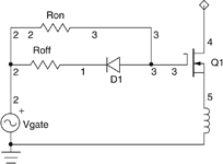
In typical hard-switched applications, different gate drive turn-on and turn-off impedances are required, as illustrated in Figure 8. As previously described, turn-on resistance is typically set to control turn-on di/dt. The turn-off impedance is set much lower, particularly for MOSFETs where the switching speed can be greatly impacted by the speed at which the VGE voltage is pulled to zero potential.
The FOM, or figure of merit, which is the gate charge QG(on) times RDS(on), is often used for comparing MOSFETs; the lower the FOM, the better the device’s performance. This comparison is only valid, however, if compared under identical conditions. That is typical parameter versus typical parameter or max versus max at the same Tj, VDS, VGS and ID.
Thermal management
One of the more critical parameters in optimising SMPS component selection is the thermal system. If the SMPS will operate in a high thermal ambient, or has a marginal heatsink, the only solution may be to select a larger die size or to parallel power devices.
Another key thermal factor is the thermal interaction between power devices. A good example is the boost diode and boost switch in a CCM boost PFC circuit. If the circuit is hard-switched then the primary switch loss is the Eon turn-on, which is predominantly a function of the boost diode. If the boost diode is closely coupled thermally to the boost switch, an interaction will occur. Eon loss in the switch will raise the boost diode temperature. This in turn will increase the diode IRRM, further increasing the switch Eon loss.
For hard-switched operating frequencies in the range of 50 kHz or greater, the cooling system often determines the choice between IGBTs and MOSFETs. If the design is below 50 kHz and sufficient cooling is available, the IGBT may be the optimum choice. However, if the boost switch losses must be spread out over a broader area requiring device paralleling, the MOSFET should be chosen since its PTC characteristics will ensure load current sharing.
Conclusions
While IGBT and MOSFET gate drive requirements are similar, subtle differences in minimum required gate drive voltage and gate drive source resistance require adjustments when switching from one device to the other. There is no across-the-board solution when using power switching devices; circuit topology, operating frequency, ambient temperature and physical size constraints all play a part in determining the optimum choice.
In ZVS and ZCS applications with minimised Eon losses, MOSFETs are capable of operating at higher frequencies because of their faster switching and lower turn-off losses. For hard-switched applications, the MOSFET parasitic body diode’s recovery characteristics can be a detriment. Conversely, since IGBT co-pack diodes are matched to the specific application, excellent soft-recovery diodes are matched with the higher-speed SMPS rated devices.
The white paper on which this article is based can be found here.
References
1. Pittet, Serge and Rufer, Alfred, ‘Analytical analysis of Quasi-Saturation Effect in PT and NPT IGBTs’, PCIM Europe 2002 http://leiwww.epfl.ch/publications/pittet_rufer_pcim_02.pdf
2. Kolar, J.W., Ertl, H. and Zach, F.C. (1998), ‘How to include the dependency of the Rds(on) of power MOSFETs on the instantaneous value of the drain current into the calculation of the conduction losses of high-frequency three-phase PWM inverters’, IEEE Trans. Ind. Electronics, Vol. 45, No.3, pp. 369–375, June 1998.
3. Stuart, T.A. and Shaoyan Ye (1994), ‘Computer simulation of IGBT losses in PFC circuits’, IEEE 4th Workshop on Computers in Power Electronics, pp.85–90, 1994.
4. Masserant, B. and Stuart, T.A., (1996), ‘Experimental verification of calculated IGBT losses in PFCs’, IEEE Transactions on Aerospace and Electronic Systems, Vol. 32, No. 3, pp. 1154–1158, July 1996.
5. Elasser, A., Parthasarathy, V. and Torrey, D. A., ‘A Study of the Internal Device Dynamics of Punch-Through and Nonpunch-Through IGBT’s Under Zero-Current Switching’, IEEE Trans. on Power Electronics, Vol. 12 No. 1, pp 21–35, January 1997.
| Tel: | +27 11 923 9600 |
| Email: | [email protected] |
| www: | www.altronarrow.com |
| Articles: | More information and articles about Altron Arrow |


© Technews Publishing (Pty) Ltd | All Rights Reserved
 printer friendly version