


Power Semiconductors are facing rising demands. Faster switching frequencies and higher operating temperatures provide a challenge for packaging and system concepts.
Notebooks of today and tomorrow require an increase of DC-DC voltage converters because of features such as HD DVD players, various network connections, and interfaces such as Bluetooth, wireless and USB. They have to be smaller, thinner and lighter.
Infineon’s answer to this trend is the introduction of products in the PowerStage 3x3 package.
PowerStage 3x3
The PowerStage 3x3 is a leadless SMD package which integrates the low-side and high-side MOSFET of a synchronous DC/DC converter into a 3,0 x 3,0 mm package outline with only 0,8 mm package height (Figure 1).
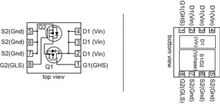
On the bottom of the package, two separate exposed pads are located which are optimised for the chip size of the low-side and the high-side MOSFET for advanced power dissipation.
Saving space dramatically
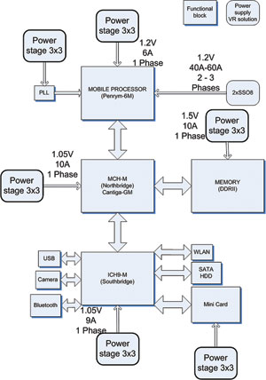
A simplified block diagram of a typical notebook-application is shown in Figure 2. Besides the power supply for the CPU, which requires high current and therefore high power dissipation capability, all other rails are in the range of 5 A to 10 A. That is where the PowerStage 3x3 fits ideally.
The typical topology for the power conversion in the above-mentioned applications is the buck converter. Today`s standard solution is realised in a 5 x 6 mm (SuperSO8) or 3 x 3 mm (S3O8) package. Figure 3 shows the comparison of the area consumption in a buck converter with one high-side and one low-side MOSFET.
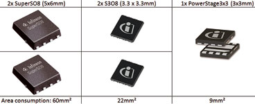
With the PowerStage3x3, designers can dramatically save space compared to two single products.
Two different products
With the BSZ0907ND and BSZ0908ND, Infineon Technologies offers two different products in the PowerStage 3x3 package. Table 1 provides a summary of the most important parameters (typical values at 4,5 V driving voltage). Both products are realised in the OptiMOS 30 V voltage class which targets voltage regulation applications in the computing and telecom segment.
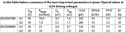
With its low Rds(on) values, the BSZ0907ND can handle 12,5 A (without airflow) and more, depending on the cooling conditions in the application. With higher Rds(on) values in the high-side and low-side MOSFET, the BSZ0908ND is designed to handle currents in the range of 5-10 A.
The Rds(on) ratio of both products is adjusted to fit a broad range of power conversions for different applications and especially for applications like mobile computing with a conversion from 21 V or 16 V down to 1,5 V.
Increasing efficiency
The QGD of the high-side MOSFET (in both products) is low in order to keep the switching losses balanced with the conduction losses and have very high peak efficiency; this is quite important especially in notebook applications where the system is working in low power range most of the time.
A low QG is realised in order to preserve high efficiency at very low load or when the system is in an idle state. This helps to maintain the battery charge for a longer time. The very low thermal resistance (55 K/W) allows the products to deliver up to 2,3 W of power; the interconnection of the chip and the pins are designed to handle 30 A, which can occur in the voltage regulation during load transients.
Top performances in the application
The PowerStage 3x3 not only offers a very compact solution for half-bridge MOSFETs itself, but also simplifies the layout of the overall buck converter. In Figure 4 an easy layout solution with the PowerStage 3x3 is shown. The area for the overall solution is 12 x 12 mm; this very dense layout is possible due to the optimised pinout of the package.
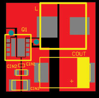
The input capacitance can be located easily between the drain of the high-side and the source of the low-side MOSFET. This minimises the parasitics of the connections. The two gates of the low-side and high-side MOSFETs can easily be connected to the driver on the bottom of the board through two small vias. The output filter can be accommodated on the right side of the package.
Efficiency measurements
With particular attention to the notebook market, some tests were performed in order to show the package’s capabilities as well as product performances. The tests are performed mainly under notebook conditions, but they can also be used as a reference for other applications.
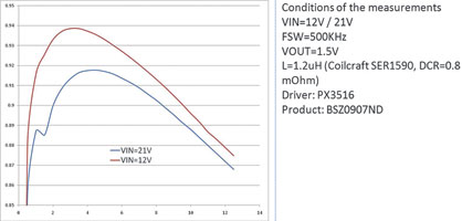
Figure 5 shows the efficiency versus output current for two different input voltages: 12 V and 21 V. In the notebook application, 12 V corresponds to the operating conditions with a battery (3 cells Li-Ion) and 21 V is related to the adaptor output voltage. In both cases the efficiency is above 90% in the range of 20% to 80% of the output load. For low load condition (0,5 A) efficiency values above 80% can be achieved.
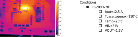
In Figure 6 the thermal capabilities of the package are shown; once a continuous current of 12,5 A is applied the top case temperature will not exceed 110°C.
In the waveforms in Figure 7, the VDS high-side MOSFET, low-side MOSFET and the input voltage are plotted. Conditions of the measurement are: VIN = 12 V, FSW = 500 kHz, VOUT = 1,5 V, L = 1,2 μH (Coilcraft SER1590, DCR = 0,8 mΩ); driver: PX3516.
The overshoot (the value of the maximum voltage during the oscillation across the device) on the low-side MOSFET is 23 V, which is below 80% of the VBDSS value specified in the datasheet. Also the damping factor of the ringing is high in order to have low noise irradiation and therefore low EMI influence. Especially for equipment with wave transmitters where many logic signals occur, this low noise irradiation provides a great benefit.
For more information contact Davis Moodley, Infineon, +27 (0)11 706 6099, www.infineon.com


© Technews Publishing (Pty) Ltd | All Rights Reserved
 printer friendly version