


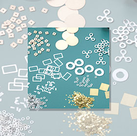
Solder preforms are used in a variety of applications that require precise amounts of solder. Preforms come in standard shapes such as squares, rectangles, washers and discs, with typical sizes ranging from 0,254 mm up to 50,8 mm, although smaller and larger sizes, as well as custom shapes, are also available. Dimensions can be held to tight tolerances to assure volume accuracy.
Selecting alloys
A wide assortment of alloys is available in liquidus temperatures that range from 47°C to 1063°C. Alloys can be indium-containing, gold-containing, lead-free, fusible or standard tin-lead, as well as many others.
Alloy selection should be based on strength and other required physical properties, as well as the preferred soldering temperature and the operating temperature of the device being soldered. A general rule is to select an alloy that melts at least 50°C higher than the operational temperature of the part being soldered.
Next, consider the materials being soldered and what solder is most compatible with them. For example, tin-based solders will scavenge the gold from gold-plated parts, forming brittle intermetallics, so indium-based solders are generally recommended in these cases. Metals and alloys have different characteristics that can affect the ease with which they can be made into different shapes and thicknesses. It is important to consider the shape of the final preform in the alloy selection process.
The operating environment of the completed assembly is also an important consideration for alloy selection. Will it operate in very high or very low temperatures, or be subjected to vibration? If so, an alloy must be chosen that will stand up to these conditions.
Selecting dimensions
The location of the solder joint and the volume of solder needed will determine the size and shape of the preform. Once the flat dimensions (diameter, length, width) have been determined, the thickness can be adjusted to achieve the desired volume of solder. Generally, for through-hole connections, add 10% to 20% to the calculated volume for a good fillet. For pad to pad joints, figure about 5% less surface area than the pad.
Each solder preform should have a burr tolerance specified; one should stay as close to standard tolerances as possible to avoid adding cost and lead time to preforms. Indium Corporation has an extensive library of sizes and shapes from which to choose, or it can create a setup specifically for a custom application. Using an existing preform size can eliminate the additional time associated with creating a new setup.
Packaging and storage
Solder preforms come in a variety of packaging options, including tape and reel. To minimise excessive handling and exposure to air and subsequent oxidation, solder preforms should be packaged according to the quantity used during a typical work shift.
Store in the original container, closed securely, in 55% RH or less and at temperatures less than 22°C. Solder preforms can also be stored in an inert atmosphere, such as a nitrogen dry box.
Shelf life
The shelf life of solder preforms is dependent on the alloy composition. Lead-free alloys, and alloys with lead content of less than 70%, have a shelf life of one year from the date of manufacture (DOM). Alloys with lead content exceeding 70% have a shelf life of six months from the DOM.
For more information contact Techmet, +27 (0)11 824 1427, [email protected], www.techmet.co.za
| Tel: | +27 11 824 1427 |
| Email: | [email protected] |
| www: | www.techmet.co.za |
| Articles: | More information and articles about Techmet |


© Technews Publishing (Pty) Ltd | All Rights Reserved
 printer friendly version