Stencil underside cleaning and manual post-cleaning
27 February 2019
Manufacturing / Production Technology, Hardware & Services
Information from kolb.
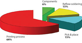
According to experts, between 60 and 70% of all defects and failures during or after the soldering process are attributable to defects in the printing process (Figure 1). In general, these are faulty solder joints, which in turn have their causes in solder paste printing mistakes. Therefore, the stencils used in the assembly process must already be cleaned during the printing process – if not, soldering errors caused by luting and bridges are inevitable.
Figure 1. Approximately 64% of process-related failures are related to deficits in the entire printing process.
Especially in the fine and ultrafine pitch range, many details are no longer visible to the naked eye (a stencil designed for wafer production can easily have more than 300 000 apertures). Microscopic carry-overs cause a noticeable loss of quality or lead to later failures or rework, which can amount to about 25% of the manufacturing costs of an assembly.
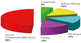
Figure 2. The stencil area alone is responsible for almost half of the total failures.
It is realistic to assume that the failure rate of 15% each during picking-and-placing and soldering would also be of a similar value for the machine printing performance, considering the use of always perfectly new and cleaned stencils. As a reverse conclusion, this means that almost 50% of process-related failures – besides wear and tear – are attributable to poor or inadequate cleaning of the relevant production tools like stencils and squeegees (Figure 2).
In order to ensure a qualified printing process in an SMD screen printer as long as possible before the stencil has to be externally machine cleaned, it is necessary to clean the underside of the stencil from flux residues already inside the screen printer.
In modern screen printers, this usually happens during the process through an automatic bottom cleaning unit, using cleaning fleeces and a suitable ready-to-use detergent. A suitable stencil cleaner for use in screen printers – such as kolb’s WipeEx SA120, which has been specially developed for this purpose – offers qualified and efficient cleaning performance due to the following factors:
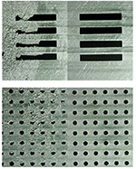
Figure 3. Stencil apertures before and after cleaning with Wipex SA 120.
• Optimal flow and wetting properties
• One-phase (aqueous, stable)
• Cleans SMD paste and SMD glue
• Cleans in contaminated state
• Fast, residue-free evaporation/ drying
• Does not change the viscosity of the adhesive
• Does not cause polymerisation (curing) of the adhesive
• No classification as a dangerous good
• Non-critical flash point (optimal >120°C)
• Biodegradable (92% after 28 days [OECD Test 301A])
• Low odour (with fresh scent)
In certain cases, manual (re)work on the stencils may be necessary; or, when it comes to cleaning squeegees by hand, to avoid carryover here too. For that kolb offers WetWipes, WipeEx’ SA120 impregnated, ready-to-use cleaning wipes with a cleaning fleece especially for stencils with fine apertures, low to no particle delivery, even soaking, and high elasticity/tear strength with high absorption of the medium or paste mixture.
World-first 016008 mm component placement
Manufacturing / Production Technology, Hardware & Services
Fuji has achieved the world’s first placement of 016008 mm (0,16 x 0,08 mm or 006 x 003 inches) size components on printed circuit boards with its SMT pick and place machine, NXTR.
Read more...Lifecycle and obsolescence: Protecting electronics through process Production Logix
Manufacturing / Production Technology, Hardware & Services
At Production Logix, we believe longevity is not accidental. It is engineered through early visibility, structured response, and disciplined execution, in partnership with our OEM customers.
Read more...Maximising squeegee quality and durability Testerion
Manufacturing / Production Technology, Hardware & Services
Transition Automation has announced two new product advancements designed to improve SMT printing performance and extend squeegee life: laser-enhanced Permalex bonding and integrated edge protectors.
Read more...NeoDen ND2 PCB screen printer ZETECH ONE
Manufacturing / Production Technology, Hardware & Services
The NeoDen ND2 PCB screen printing machine is a fully automatic stencil printer designed to deliver precise and consistent solder paste application in modern SMT production environments.
Read more...Understanding the BGA rework process Techmet
Manufacturing / Production Technology, Hardware & Services
BGA rework is a highly technical process that involves removing the faulty component, preparing the circuit board, and installing a new or repaired device, while maintaining the integrity of the printed circuit board.
Read more...Flexible three-process reflow soldering system Truth Electronic Manufacturing
Manufacturing / Production Technology, Hardware & Services
By combining multiple soldering technologies within a single system, the Vision TripleX system enables manufacturers to adapt easily to different assembly requirements, board designs, and production volumes.
Read more...Inline vapour phase soldering for high-volume production MyKay Tronics
Manufacturing / Production Technology, Hardware & Services
The VP2200-100 vacuum inline vapour phase soldering system from ASSCON is designed for fully automated, high-volume electronics manufacturing where process consistency and solder joint quality are critical.
Read more...Global electronics solutions since 1964 IMP Electronics Solutions
Manufacturing / Production Technology, Hardware & Services
Over more than six decades, IMP Electronics Solutions has built a reputation for technical expertise, reliable supply chains, and strong partnerships with both customers and manufacturing partners.
Read more...Driving excellence in electronics manufacturing Jemstech
Editor's Choice Manufacturing / Production Technology, Hardware & Services
Jemstech’s reputation for disciplined execution and client-focused service has earned it strong loyalty from companies operating in demanding industries.
Read more...When do you need Nitrogen in reflow? Truth Electronic Manufacturing
Manufacturing / Production Technology, Hardware & Services
Nitrogen in reflow soldering is often seen as a performance enhancer, offering improved wetting, shinier joints, and fewer defects. But it is not always necessary.
While every effort has been made to ensure the accuracy of the information contained herein, the publisher and its agents cannot be held responsible for any errors contained, or any loss incurred as a result. Articles published do not necessarily reflect the views of the publishers. The editor reserves the right to alter or cut copy. Articles submitted are deemed to have been cleared for publication. Advertisements and company contact details are published as provided by the advertiser. Technews Publishing (Pty) Ltd cannot be held responsible for the accuracy or veracity of supplied material.


 printer friendly version