Manufacturing / Production Technology, Hardware & Services


X-ray dose considerations

27 March 2019 Manufacturing / Production Technology, Hardware & Services

The benefits of using X-ray technology in the electronics industry to inspect printed circuit board assemblies are well proven.

This article summarises X-ray radiation dose, and the techniques that can be employed to reduce radiation exposure to samples in a Nordson Dage Quadra X-ray inspection system.

Quadra X-ray geometry

First we need to consider how the Quadra X-ray inspection system works. Quadra allows the internal structure of samples to be seen by shining X-ray light through a sample (Figure 1). This creates a shadow image that is detected in real-time using a high-resolution Aspire flat panel X-ray detector. The darkness of the shadow cast by any point in the sample depends on how much X-ray light has been absorbed by that part of the sample.

Figure 1. Quadra X-ray tube, sample and detector geometry shown at low magnification (left) and high image magnification (right).

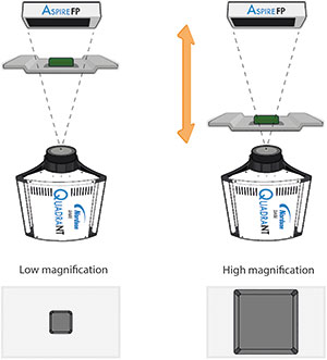
High image magnification is used to see smaller features clearly. This is achieved by moving the sample closer to the X-ray tube. For the highest magnification, the sample tray is lowered to the top of the X-ray tube.

Figure 2. Oblique viewing angles are achieved by moving the detector in a hemisphere around the sample.

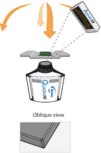
Viewing the sample from different angles allows more defects to be observed. The Aspire flat panel detector moves around two oblique axes to allow this. X-rays from the QuadraNT X-ray tube are emitted over a wide cone angle so there are plenty of X-rays available off-axis.

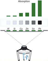
Different materials absorb radiation to differing degrees (Figure 3). Lead is very good at absorbing X-ray radiation which is why it’s used to shield the X-ray cabinet. Silicon and aluminium are relatively poor at absorbing X-rays so images tend to be very bright. Tin and copper, commonly used in solder, are somewhere in between.

Figure 3. X-ray absorption by different materials of the same thickness.

The shadow created at any point also depends on the voltage and power used to drive the X-ray tube (Figure 4). An X-ray tube operating at a voltage of 80 kV creates X-rays over the entire energy range up to 80 keV. Increasing the voltage to 160 kV doubles the X-ray output energy range from 80 keV to 160 keV.

Figure 4. X-ray photon energy output for different tube voltage and power settings.

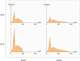
Increasing the tube power increases the number of X-rays emitted at every point over the range. In general, higher energy X-rays are more likely to pass through a sample than lower energies. High energy beams are useful for looking at thick samples, or materials that strongly absorb X-rays, for example lead. Lower energy X-rays are better for thinner samples, or materials that weakly absorb X-rays, for example copper or silicon.

What is X-ray dose?

The X-ray dose for any part of the sample is a measure of the X-ray energy absorbed per unit mass, and is measured in units of gray (Gy), where

1 Gy = 1 J/kg = 100 rad.

Since different materials absorb incoming X-rays with differing efficiency, their absorbed dose will vary when placed in the same X-ray beam. A material like lead, which absorbs X-rays well and casts a dark shadow in an image, will absorb a higher dose than a material like silicon which absorbs X-rays weakly.

The absorbed dose also varies with:

• Distance to the X-ray source: The amount of X-ray radiation reduces as 1/r² in the same way a light appears brighter the closer you are to it.

• Time in X-ray source: X-ray dose is cumulative so the longer spent in the X-ray beam, the higher the absorbed dose.

• X-ray tube output: The higher the tube power or voltage, the larger the absorbed dose.

How to reduce sample dose

Reducing the magnification used and minimising the time the X-ray tube is switched on are effective ways to reduce X-ray dose. Quadra’s low dose mode can be used to switch X-rays off when it detects the sample is no longer being manipulated.

Figure 5. X-ray photon energy output without (top) and with (bottom) additional filtering. The energies below 30 keV do not contribute to the final image but still contribute to absorbed dose.

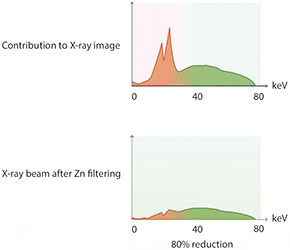
Another method is to filter out lower energy X-rays (Figure 5). These X-rays do not contribute to the final image for two reasons:

Figure 6. Absorbed dose and image quality for a typical silicon sample with filtering tray (left) and without (right).

• Absorption by sample: At low energies, particularly below 20 keV, X-rays are strongly absorbed by most samples. They contribute to sample dose, but are less likely to make it through the sample to the X-ray detector.

• Detector sensitivity: Flat panel X-ray detectors, like AspireFP, are insensitive to X-rays below ~20 keV. Any X-rays that manage to pass through the sample have a lower likelihood of being detected.

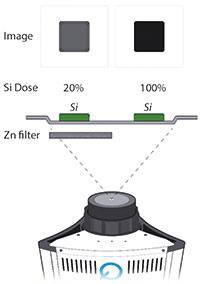
Filtering out low energy X-rays is an effective way to reduce sample dose without compromising image quality. A filtering sample tray is available for Quadra which incorporates zinc strips to absorb low energy X-rays while letting higher powers pass through to the sample. This can reduce overall X-ray dose by up to 80% (Figure 6).

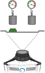
Masking is a simple way of reducing X-ray dose for any components on a board that do not need to be inspected at all by X-ray. A portion of dense material, for example lead, can be attached to the sample tray immediately below the sample to mask the sensitive component from X-rays.

Quadra includes a dose calculation tool that tracks the average dose acquired by the whole sample during inspection. For the most accurate results, the tool can be calibrated by measuring X-ray dose in the path of the X-ray beam before and after the sensitive component (Figure 7).

Figure 7. Sample absorbed dose can be measured by measuring 
and subtracting dose with and without sample present.
Figure 7. Sample absorbed dose can be measured by measuring and subtracting dose with and without sample present.

Getting better images from thin samples

High energy X-rays are poorly absorbed by thin samples, or by weakly absorbing materials such as silicon or aluminium. Medium energy X-rays give the best image contrast for these samples. However, these energies are typically between 30 and 80 kV and are attenuated by ~90% by the standard aluminium sample tray.

Figure 8. Thin sample tray allows higher contrast images at lower X-ray energies.

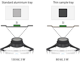
A thin sample tray is available for Quadra which is manufactured from a thin layer of carbon fibre instead of a thicker layer of aluminium. This allows 10 times more medium energy X-rays to pass through, creating clearer images with better contrast.


Credit(s)


Share this article:
Share via emailShare via LinkedInPrint this page

Further reading:

Outscale your competition
Manufacturing / Production Technology, Hardware & Services
Attendees will be able to explore the benefits of AMD Kintex UltraScale+ Gen 2 FPGAs in high-performance Pro AV, test & measurement, industrial, and medical applications.

Read more...
MTN SA Foundation drives youth pathways into the digital economy
Manufacturing / Production Technology, Hardware & Services
The MTN SA Foundation, in partnership with Helios Towers and Datacomb Development Hub, has launched the MTN–Helios Towers 12-month ICT Learnership Programme, a pathway that takes young South Africans from digital training into real workplace experience.

Read more...
Downstream demand, system reliability, and the expanding role of engineering-led distribution
Manufacturing / Production Technology, Hardware & Services
[Sponsored] As South Africa’s semiconductor demand continues to be shaped by downstream system deployment rather than upstream fabrication, the importance of engineering-led distribution will continue to grow.

Read more...
The impact of harsh environments and ionic contamination on post-reflow circuit assemblies
MyKay Tronics Manufacturing / Production Technology, Hardware & Services
There is well documented historical proof that post-reflow circuit assemblies, when subjected to harsh environments, are particularly vulnerable to failure mechanisms, but modern electronic assemblies are far more susceptible to this phenomenon.

Read more...
Engineering copper grain structure for high-yield hybrid bonding in 3D packaging
Testerion Editor's Choice Manufacturing / Production Technology, Hardware & Services
The way copper grains are sized and distributed forms the metallurgical foundation of hybrid bonding, enabling lower bonding temperatures, greater reliability, and stable grain structures throughout integration.

Read more...
Understanding solder dross: causes and control strategies
Truth Electronic Manufacturing Editor's Choice Manufacturing / Production Technology, Hardware & Services
Dross formation is an inevitable consequence of wave soldering. It occurs when molten solder comes into contact with oxygen, forming metal oxides that float on the surface of the solder bath. Over time, this oxidation byproduct accumulates and must be removed to maintain solder quality and process consistency.

Read more...
Non-destructive techniques for identifying defects in BGA joints – TDR, 2DX, and cross-section-SEM comparison
MyKay Tronics Manufacturing / Production Technology, Hardware & Services
This whitepaper reports the results of a comparison of the following techniques: TDR, automatic X-ray inspection (AXI), transmission X-ray (2DX), cross-section/SEM, and Dye & Pry.

Read more...
Implications of using Pb-free solders on X-ray inspection of flip chips and BGAs
MyKay Tronics Manufacturing / Production Technology, Hardware & Services
With the move to Pb-free soldering, most of the attention has been paid to reflow temperatures, component compatibility, and reliability concerns, but the implications for inspection, particularly X-ray inspection, are equally important and often underestimated.

Read more...
The causes of solder balls in robotic soldering
Manufacturing / Production Technology, Hardware & Services
Solder balls (also known as solder splatter) are a major concern in many production sites as they may potentially cause shorts, leading to long-term impacts on product reliability.

Read more...
Material challenges for superconducting quantum chips
Manufacturing / Production Technology, Hardware & Services
To achieve the scalable and repeatable production of superconducting circuits for quantum technology products, players in the industry are leveraging semiconductor fabrication techniques.

Read more...


While every effort has been made to ensure the accuracy of the information contained herein, the publisher and its agents cannot be held responsible for any errors contained, or any loss incurred as a result. Articles published do not necessarily reflect the views of the publishers. The editor reserves the right to alter or cut copy. Articles submitted are deemed to have been cleared for publication. Advertisements and company contact details are published as provided by the advertiser. Technews Publishing (Pty) Ltd cannot be held responsible for the accuracy or veracity of supplied material.


© Technews Publishing (Pty) Ltd | All Rights Reserved