


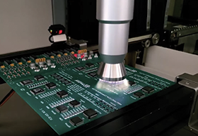
Plasma treatment involves exposing PCBs to an ionised gas, known as plasma, to alter the surface at a molecular level. This process is typically used to:
• Remove contaminants and improve cleanliness.
• Increase surface energy for better adhesion of coatings, solder masks, or adhesives.
• Modify surface properties for advanced manufacturing needs.
Despite these advantages, several risks must be managed to ensure safe and effective plasma application in EMS.
1. Excessive etching or surface damage
Cause: Over-treatment caused by prolonged exposure, excessive energy, or unsuitable gas selection.
Risk: May result in thinning of copper traces, microcracks, or even the erosion of delicate circuit features, compromising electrical performance and product reliability.
Solution: Carefully optimise treatment time and energy levels based on PCB material and design.
2. Contaminant residue
Cause: Contamination in the plasma chamber or low-quality process gases.
Risk: Residual contaminants left on the PCB surface can interfere with electrical performance, particularly in high-frequency applications.
Solution: Regular maintenance of plasma equipment and the use of high-purity process gases can minimise contamination risks.
3. Dielectric layer degradation
Cause: High-energy plasma interaction with the PCB’s insulation layers, such as solder masks or dielectric materials.
Risk: Damage to the dielectric layer reduces insulation resistance, increasing the risk of short circuits or dielectric breakdown.
Solution: Test and adjust plasma parameters to ensure compatibility with the dielectric materials used in PCBs.
4. Thermal stress
Cause: Plasma processes generating localised heat, particularly during prolonged treatment.
Risk: Thermal stress may lead to PCB warping, delamination of layers, or pad lifting.
Solution: Implement precise process controls to manage temperature and minimise thermal impact.
5. Electrostatic discharge (ESD)
Cause: Plasma processes can induce static electricity, especially in poorly grounded systems.
Risk: Static discharge can damage sensitive electronic components on the PCB.
Solution: Use ESD-safe equipment and ensure proper grounding during plasma treatment.
6. Latent structural damage
Cause: Microscopic cracks or imperfections introduced during plasma treatment.
Risk: These latent defects can propagate under stress during product operation, leading to eventual PCB failure.
Solution: Conduct quality inspections and tests after plasma treatment to detect and address hidden issues.
7. Chemical reactions from improper gas selection
Cause: The use of incompatible or contaminated gases during plasma treatment.
Risk: May result in unwanted chemical byproducts or surface modifications that degrade adhesion or electrical performance.
Solution: Choose gases carefully and ensure they are free from impurities or moisture.
Plasma treatment has become a cornerstone of modern EMS production, enabling precise surface preparation for complex PCB designs. However, unaddressed risks can lead to defects, reduced reliability, and increased production costs. By identifying and mitigating these hazards, EMS factories can ensure plasma processes deliver consistent results without compromising PCB quality. This is accomplished by optimising parameters, maintaining equipment, and implementing robust monitoring systems, allowing EMS factories to maximise the benefits of plasma treatment while minimising its potential dangers.
| Tel: | +27 11 869 0049 |
| Email: | [email protected] |
| www: | www.mykaytronics.co.za |
| Articles: | More information and articles about MyKay Tronics |


© Technews Publishing (Pty) Ltd | All Rights Reserved
 printer friendly version