


Electronics manufacturers worldwide are moving to lead-free solders for a variety of reasons that include environmental concerns and compliance with impending regulatory legislation. The development of practical lead-free alloys and flux chemistries, as well as more sophisticated soldering equipment, have made lead-free soldering a process whose time has come, and one which can be implemented successfully at the production level.
Why the '5 steps to successful lead-free soldering'?
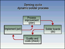
Successful implementation of lead-free soldering requires careful, well thought-out planning, as well as rigorous process monitoring to ensure quality and process control. '5 steps to successful lead-free soldering' is a guide for those who are responsible, interested or confronted with the implementation of lead-free wave and/or reflow soldering. The five steps are based upon modern techniques, (eg, problem-solving/process-improvement models (plan; do; check; act); quality engineering, design of experiments, and statistical process control).
Following these steps will lead to successful lead-free soldering for a robust, repeatable lead-free soldering process that will deliver consistent high yields. The goal is to continue where most lead-free papers stop, ie, at the point of beginning to actually solder lead-free. Many recently published papers discuss legislation, marketing, temperature, and alloy selection issues, but none describe how to actually implement the process. What must be done and investigated before the first lead-free soldered boards leave the assembly line? How can the new process be controlled and improved after implementation?
Studies plus experience
Today, knowledge of lead-free soldering is based upon feasibility studies of several consortia, wetting balance tests, university investigations, and only a small part on real lead-free soldering in the production environment. Most of the companies who have been soldering with lead-free alloys for two years or more are automotive or other (special) applications, where assemblies are subjected to temperatures in excess of 150°C or higher. The input and experiences of these companies teaches us more about issues such as solder contamination, yields, parts wear, costs, board warpage and process control aspects, where feasibility and other studies help us with material selections.
Step 1. Select the right materials and equipment
From alloy and flux selection to necessary equipment capabilities: This means not only selecting the solder alloys or paste, but also the flux, board materials and finishes as well as the component packaging material and finish.
In the lead elimination route we can differentiate three phases:
* Lead-free solder paste (reflow) and alloy (wave). The materials and technologies are currently available.
* Eliminate halogenated flame retardants from board materials with lead-free board finishes. Board material must be able to withstand higher temperatures.
* Components' lead-free finish material is dictated by the lead-free solder alloy/paste materials selection. The plastics and other component materials should have a higher heat resistance.
Define wave solder machine requirements: Fluxer application and preheat configuration must be determined depending on flux specification and required process temperatures. The wave configuration and contact times will depend on the solder joint quality as a result of solderability of the selected lead-free alloy.
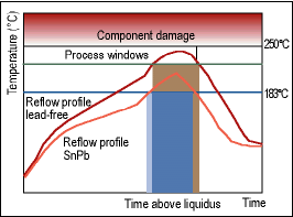
Define the reflow machine requirements: The heating method must be determined. The heating and cooling length, will be defined by a number of factors like; required machine throughput, board dimensions, distance between boards, required board exit temperature and the temperature profile based on solder paste and components specifications.
Step 2. Define the process
Define process parameters and conduct Taguchi experiments and data analysis: A Taguchi method is used to make the process minimally sensitive to variation, to find the optimum settings, and determine the sensitivity of the control parameters to variations in the process.
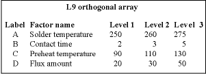
In a brainstorm stage, the problems, objectives, output characteristics and measuring methods are designed for a lead-free experiment. The selection of the control parameters and the way to quantify the results of the experimental runs are discussed. After the experiment, the data should be examined against the criteria of the output characteristics. The paper champion from the experiment must be verified by running a confirmation.
Step 3. Develop a robust process
Collect and analyse data, do the homework, and get the 'bugs' out of the process: The third step continues with the optimal control parameter settings from the experiment. The product is soldered for a longer period of time with these settings. The robustness of the process must be monitored. It is important to see if the process is stable after a number of hours, or if there is drift, which will result in trends in the SPC (statistical process control) charts. Exhaust and temperature conditions must be verified. The reliability and the yields need to be compared with the data of the traditional SnPb process. If the product quality is acceptable for a longer pre-production period and the machine meets the requirements for the new process, the process is ready for production release.
Until now, all tests could be done on a beta-site or a standalone machine. Now the organisation prepares to switch over the production line. This means that a time schedule has to be made, parts must be ordered, procedures written, and personnel must be trained.
Step 4. Implement lead-free manufacturing
Begin production, monitor the process carefully and make needed changes as you go: For wavesoldering, the installation of a new solder pot is required. The alternative is to drain the solder pot and purge it with pure tin. For the conveyor, an additional board support can be an option. In case of changing flux type, new foam tube or other spray nozzles may be required. The spray pattern and flux penetration needs to be reviewed. Since the alloys are more expensive, the use of nitrogen is more important. The amount of dross will be reduced and less aggressive fluxes can be applied. Heat profiles and contact times should be verified before the process is ready for production start.
For reflow soldering, the process may require extra cooling or adding a flux management system in order to limit the emission of residues. Although nitrogen adds more costs to the process, wetting will be improved and a less aggressive flux can be used.
Once all preparations are made, the production can start. Follow the quality procedures and make SPC charts to visualise the process, as well as product variation.
Step 5. Control and improve the process
Constant follow-up, monitoring, and data analysis keeps your process under control: Run the process and monitor the quality. The soldering process is always dynamic and continuously changing. Costs of flux, alloys, dross, nitrogen consumption, rework and energy should be calculated and compared to the traditional SnPb process. The nitrogen consumption (amount versus dross production) should be a part of the cost analysis.
Research and development will continue and therefore new materials (flux, alloys, paste, components, and board materials) should be examined every now and then. Improvements should be evaluated and implemented if necessary. All improvements are aimed at reducing variation and increasing the quality and productivity of the process.
In order to help companies successfully implement lead-free soldering, Zetech is hosting a one-day Lead-free Process and Soldering Conference in Johannesburg, Durban and Cape Town. For more information contact Bianca Loizides, 011 789 3230, [email protected]
| Tel: | +27 11 609 1244 |
| Email: | [email protected] |
| www: | www.zetech.co.za |
| Articles: | More information and articles about ZETECH ONE |


© Technews Publishing (Pty) Ltd | All Rights Reserved
 printer friendly version