Manufacturing / Production Technology, Hardware & Services


The significance of the stencil printing process

13 May 2009 Manufacturing / Production Technology, Hardware & Services

I still remember an incident that happened a few years ago, when I was called out to a customer to look at a ‘problem’ on their pick-and-place machine, where it was ‘throwing the components around’. I noticed that the components did not stay in the position where they were placed and found that the problem was in fact dried out solder paste. The dried out solder paste was not sticky enough to hold the components in place, and the result was components ‘jumping’ around on the PCB during the placement process.

The real cause of the problem was that the operators were printing more PCBs than the pick-and-place machine could process in a normal shift. The PCBs were then stored in the solder paste fridge overnight, and processed the next morning, resulting in dried out solder paste and ‘components jumping around’. Though this is an extreme case of problems related to the stencil printing process, it is a good example of how problems in printing can cause problems further down the line. Many experts in the field of SMT production have said that up to 70% of all problems in the SMT process are related to the stencil printing process. If there is one area where good process engineering can have a significant impact on the overall quality of the SMT process, then it is the stencil printing process.

Dirty stencil
Dirty stencil

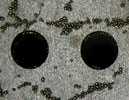
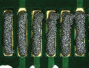
The first step towards good printing is a good stencil design. Successful process engineers understand the effect that aperture size and stencil thickness have on the printing process. Too much solder paste causes bridging, and too little solder paste causes insufficient solder – it is that simple, but I am not convinced that enough effort is being put towards good stencil design in South Africa. I have seen many problems caused by a lack in stencil design, and too often the response is ‘the buyer is responsible for ordering stencils’.

Damaged stencil
Damaged stencil

Good solder paste management is critical in achieving a good print. Many solder paste suppliers recommend storing solder paste in a fridge at 6–8°C. It is important to have a system in place to ensure that solder paste is removed from the fridge approximately 24 hours prior to use, to ensure that it reaches room temperature before use. Placing a tub of solder paste on the reflow oven to let it ‘heat up’ is not the best option.

Bad printing caused by worn parts on the stencil printer

One of the major causes of printing related problems is lack of maintenance of both the stencil printer and the stencil. A regular inspection and replacement routine will ensue that you are using a stencil which is in good condition. Ensuring that squeegee blades and PCB clamping mechanism are in good condition will go a long way towards ensuring a good printing process. The cost of replacing damaged stencils, squeegee blades or PCB clamps could typically be less than the costs incurred in rework caused by badly damaged stencils and printer parts.

Good printing
Good printing

Believe it or not, the one thing that is frequently overlooked when fault finding the SMT process is cleanliness of the stencil and the stencil printer. Dried out solder paste on the PCB support pillars and PCB clamping mechanism can cause the PCB to be elevated and thus cause an uneven print. Thorough cleaning of the stencil after every shift will ensure clean apertures and good solder paste release. Solder paste left in the stencil apertures will build up over time, and cause problems. Whether you use an automated or a manual stencil cleaning process, it is always worthwhile to do regular checks of the stencil apertures, to ensure that your stencil cleaning process is effective.

Finally, the proof is in the pudding. The simplest way to ensure that your printing process remains under control is to look at the results. There is a variety of automated equipment available in the market to inspect your solder paste print before it goes into the pick and place machine, and where this kind of equipment is not yet available, it is good practice to take a sample of a printed PCB from the production line at regular intervals, inspecting it under a microscope.

Investing time to ensure that the solder paste printing process is under control, can save a lot in rework costs further down the line. The accompanying figures show some commonly occurring stencil related problems.


Share this article:
Share via emailShare via LinkedInPrint this page

Further reading:

Outscale your competition
Manufacturing / Production Technology, Hardware & Services
Attendees will be able to explore the benefits of AMD Kintex UltraScale+ Gen 2 FPGAs in high-performance Pro AV, test & measurement, industrial, and medical applications.

Read more...
MTN SA Foundation drives youth pathways into the digital economy
Manufacturing / Production Technology, Hardware & Services
The MTN SA Foundation, in partnership with Helios Towers and Datacomb Development Hub, has launched the MTN–Helios Towers 12-month ICT Learnership Programme, a pathway that takes young South Africans from digital training into real workplace experience.

Read more...
Downstream demand, system reliability, and the expanding role of engineering-led distribution
Manufacturing / Production Technology, Hardware & Services
[Sponsored] As South Africa’s semiconductor demand continues to be shaped by downstream system deployment rather than upstream fabrication, the importance of engineering-led distribution will continue to grow.

Read more...
The impact of harsh environments and ionic contamination on post-reflow circuit assemblies
MyKay Tronics Manufacturing / Production Technology, Hardware & Services
There is well documented historical proof that post-reflow circuit assemblies, when subjected to harsh environments, are particularly vulnerable to failure mechanisms, but modern electronic assemblies are far more susceptible to this phenomenon.

Read more...
Engineering copper grain structure for high-yield hybrid bonding in 3D packaging
Testerion Editor's Choice Manufacturing / Production Technology, Hardware & Services
The way copper grains are sized and distributed forms the metallurgical foundation of hybrid bonding, enabling lower bonding temperatures, greater reliability, and stable grain structures throughout integration.

Read more...
Understanding solder dross: causes and control strategies
Truth Electronic Manufacturing Editor's Choice Manufacturing / Production Technology, Hardware & Services
Dross formation is an inevitable consequence of wave soldering. It occurs when molten solder comes into contact with oxygen, forming metal oxides that float on the surface of the solder bath. Over time, this oxidation byproduct accumulates and must be removed to maintain solder quality and process consistency.

Read more...
Non-destructive techniques for identifying defects in BGA joints – TDR, 2DX, and cross-section-SEM comparison
MyKay Tronics Manufacturing / Production Technology, Hardware & Services
This whitepaper reports the results of a comparison of the following techniques: TDR, automatic X-ray inspection (AXI), transmission X-ray (2DX), cross-section/SEM, and Dye & Pry.

Read more...
Implications of using Pb-free solders on X-ray inspection of flip chips and BGAs
MyKay Tronics Manufacturing / Production Technology, Hardware & Services
With the move to Pb-free soldering, most of the attention has been paid to reflow temperatures, component compatibility, and reliability concerns, but the implications for inspection, particularly X-ray inspection, are equally important and often underestimated.

Read more...
The causes of solder balls in robotic soldering
Manufacturing / Production Technology, Hardware & Services
Solder balls (also known as solder splatter) are a major concern in many production sites as they may potentially cause shorts, leading to long-term impacts on product reliability.

Read more...
Material challenges for superconducting quantum chips
Manufacturing / Production Technology, Hardware & Services
To achieve the scalable and repeatable production of superconducting circuits for quantum technology products, players in the industry are leveraging semiconductor fabrication techniques.

Read more...


While every effort has been made to ensure the accuracy of the information contained herein, the publisher and its agents cannot be held responsible for any errors contained, or any loss incurred as a result. Articles published do not necessarily reflect the views of the publishers. The editor reserves the right to alter or cut copy. Articles submitted are deemed to have been cleared for publication. Advertisements and company contact details are published as provided by the advertiser. Technews Publishing (Pty) Ltd cannot be held responsible for the accuracy or veracity of supplied material.


© Technews Publishing (Pty) Ltd | All Rights Reserved