24 October 2001Manufacturing / Production Technology, Hardware & Services
Information from Zetech
Flip chip technology is providing PCB designers with a myriad of options for increasing processing speed while reducing substrate area. Whether assembled into BGA packages or directly onto the substrate as a DAC (direct chip attach), flip chip technology is increasing the demands on electronics manufacturers for better control of material deposition in the flip chip, underfill process.
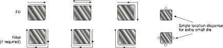
Figure 1. A variety of dispense fill and fillet patterns can be used to facilitate material flow under the chip
Shock, moisture and connectivity are key considerations in creating a reliable flip chip assembly. A proper underfill stabilises the chip's connection to the substrate and reduces the number of boards and packages requiring rework.
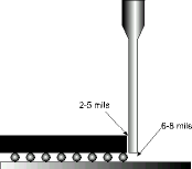
First, material is dispensed along one or more sides of the chip. The material typically is pre-heated to 40-60°C via a syringe heater to reduce material viscosity. To dispense the material, the needle is positioned 2-5 mils from the chip and 6-8 mils from the substrate. This allows the material to flow under the chip to prevent ploughing material onto the top of the chip or build up around the sides of the needle.
Figure 2. The needle is positioned 2–5 mils from the chip and 6–8 mils from the substrate to prevent dispense material from ploughing onto the top of the chip or build up around the sides of the needle
During the underfill phase, complete and precise coverage under the chip is crucial. If too much material is dispensed, the operator will flood the die in a BGA package or run the underfill material into other chips on a high-density assembly. Too little material results in uneven coverage and a less stable package. In this phase, the substrate is heated to 70-100°C to enhance capillary action under the chip and to assist material in releasing from the tip of the needle. Heat is applied through a heated vacuum fixture.
Finally, a fillet can be dispensed along one or more sides of the chip, sealing the underfill material and further protecting the chip. Again, the needle must be positioned precisely on the X, Y and Z-height coordinates to ensure accurate deposition. The package or assembly is then sent through final convection heating at 70-100°C to stabilise the material prior to batch curing.
GPD manufactures the DS series of liquid dispensing equipment for micro volume flip chip underfill applications. The systems offer less than 1 mil location accuracy in the dispense area using a traceable glass plate procedure. Pre-dispense, dispense and post-dispense heating is controlled within ±3°C.
World-first 016008 mm component placement
Manufacturing / Production Technology, Hardware & Services
Fuji has achieved the world’s first placement of 016008 mm (0,16 x 0,08 mm or 006 x 003 inches) size components on printed circuit boards with its SMT pick and place machine, NXTR.
Read more...Lifecycle and obsolescence: Protecting electronics through process Production Logix
Manufacturing / Production Technology, Hardware & Services
At Production Logix, we believe longevity is not accidental. It is engineered through early visibility, structured response, and disciplined execution, in partnership with our OEM customers.
Read more...Maximising squeegee quality and durability Testerion
Manufacturing / Production Technology, Hardware & Services
Transition Automation has announced two new product advancements designed to improve SMT printing performance and extend squeegee life: laser-enhanced Permalex bonding and integrated edge protectors.
Read more...NeoDen ND2 PCB screen printer ZETECH ONE
Manufacturing / Production Technology, Hardware & Services
The NeoDen ND2 PCB screen printing machine is a fully automatic stencil printer designed to deliver precise and consistent solder paste application in modern SMT production environments.
Read more...Understanding the BGA rework process Techmet
Manufacturing / Production Technology, Hardware & Services
BGA rework is a highly technical process that involves removing the faulty component, preparing the circuit board, and installing a new or repaired device, while maintaining the integrity of the printed circuit board.
Read more...Flexible three-process reflow soldering system Truth Electronic Manufacturing
Manufacturing / Production Technology, Hardware & Services
By combining multiple soldering technologies within a single system, the Vision TripleX system enables manufacturers to adapt easily to different assembly requirements, board designs, and production volumes.
Read more...Inline vapour phase soldering for high-volume production MyKay Tronics
Manufacturing / Production Technology, Hardware & Services
The VP2200-100 vacuum inline vapour phase soldering system from ASSCON is designed for fully automated, high-volume electronics manufacturing where process consistency and solder joint quality are critical.
Read more...Global electronics solutions since 1964 IMP Electronics Solutions
Manufacturing / Production Technology, Hardware & Services
Over more than six decades, IMP Electronics Solutions has built a reputation for technical expertise, reliable supply chains, and strong partnerships with both customers and manufacturing partners.
Read more...Driving excellence in electronics manufacturing Jemstech
Editor's Choice Manufacturing / Production Technology, Hardware & Services
Jemstech’s reputation for disciplined execution and client-focused service has earned it strong loyalty from companies operating in demanding industries.
Read more...When do you need Nitrogen in reflow? Truth Electronic Manufacturing
Manufacturing / Production Technology, Hardware & Services
Nitrogen in reflow soldering is often seen as a performance enhancer, offering improved wetting, shinier joints, and fewer defects. But it is not always necessary.
While every effort has been made to ensure the accuracy of the information contained herein, the publisher and its agents cannot be held responsible for any errors contained, or any loss incurred as a result. Articles published do not necessarily reflect the views of the publishers. The editor reserves the right to alter or cut copy. Articles submitted are deemed to have been cleared for publication. Advertisements and company contact details are published as provided by the advertiser. Technews Publishing (Pty) Ltd cannot be held responsible for the accuracy or veracity of supplied material.


 printer friendly version