


Continued from previous article, 21 February 2007
It all began in 2006 with Bob Willis and his team’s visit to SA and, in particular, the Lead-Free seminar I attended in Stellenbosch. My first article was published in January 2007 and was inspired by all the activities and efforts brought about by the overseas and local experts. I thought it appropriate to add a small contribution myself.
After a period of silence and coincidentally - or is it really coincidence? - a follow-up visit by Keith Bryant of the UK SMART Group, I was prompted again to carry on with a follow-up article on myths and beliefs. Those curious enough and having the time could perhaps have a look at the Dataweek article in the 21 February issue.
I cannot stress enough how important it is for all of us to start talking the same language when it comes to electronic assembly and soldering. It prevents misunderstandings and eliminates or reduces the misdirection of expensive funding required in a modern electronics assembly plant.
Not long after the article on myths was published, I came across 'experienced' assembly staff and operators merrily chatting about a 'dry-joint' here and a 'dry-joint' there. Did the technicians, engineers or in-house trainers not explain to them that the 'dry-joint' should have died 45 years ago? If it had been close to Christmas I would have excused them as having been submitted to Santa Claus and other myths. However, these were operators and assemblers with 20 to 30 years of 'experience'. They should know better by now. Let me briefly refresh the subject and share one of the definitions I really like: according to Trice and Beyer (1984), I quote: "Myths can also be defined as a dramatic narrative of imagined events, usually to explain origins or transformations of something. It also reflects an unquestioned belief about the practical benefits of certain techniques and behaviour that is not supported by demonstrated facts".
If in doubt, do not mumble but go to the -'good book'. In our case a good book would be the IPC-T-50G 'Terms and Definitions for Interconnecting and Packaging Electronic Circuits'. This book also contains most of the commonly used acronyms like RwoH (reliability without hermeticity), SMOGB (solder mask over gold body) and many others. Its main purpose is to enlighten us on the terms and definitions per se. One could argue that the mythical 'dry-joint' should be found between drag soldering and dry glass (clad laminate). But no, it is not there. If you ever attended an IPC course like IPC-A-610D, J-STD-001D, IPC-7711 or IPC-7721, a trainer worth his salt should have given you the 133 page IPC-T-50G manual either in print or on electronic format. If it is available in your company, do me a favour, and please consult it. Those who can prove the existence of a dry joint definition in IPC literature will be personally rewarded by me.
What is the fuss? My master IPC trainer from Denmark, Finn, briefly reacted when I asked him the question in 2004. His answer: "Eddy, it does not exist" and he carried on with more important aspects of the course. To me it still remains a mystery why so many people are still using it. This brings us to a second but no less important misbelief or misunderstanding: the confusion between non-wetting and de-wetting. This strictly does not belong under the heading of 'Myths', but can be dealt with under 'beliefs'.
It is amazing how one finds this confusion to be mostly prevalent in the electronics assembly industry. Ask people about wetting, non-wetting and de-wetting and most will be standing and gazing or mumbling something. I personally do not know of any industry that seems to be so ill prepared when it comes to the hands-on practical application of electronics. My discussions with some of the professors and academic staff at the University of Pretoria many years ago revealed that these institutions have not the time, staff, nor the programmes available to equip the modern engineer with sufficient hands-on experience. Technical colleges do include some of the SAQA Unit standards in their courses, however I have been through most of these Unit Standards and found some of them incomplete and with a few errors. Let us hope the continuous reviews by the SGBs (standards generating bodies) pick those up and improve on this situation.
What is it with the non-wetting and de-wetting issues? Should we really care so much and not just fix the problem and get on with the job? Would the worker be happy if we gave him or her a shovel instead of a spade? Why bother?
Let us first have a look at what is meant by non-wetting and de-wetting, and where else would we find a better definition than in IPC-T-50G mentioned earlier? Nonwetting - one word - (solder) p. 61 code 75.1189 in IPC-T-50G: "The inability of molten solder to form a metallic bond with the basis metal". How can one see the difference between good wetting and non-wetting? Usually by the shape of the solder fillet that was formed after the soldering process has been completed. It is a smooth unbroken fillet of a concave (hollow) shape indicating that good wetting has taken place - see Figure 1. Non-wetting can be seen by the formation of a bulbous joint having a convex shape. De-wetting is another issue altogether.

The definition of de-wetting (dewetting, one word in IPC) can be found on page 28 of IPC-T-50G, Code 97.0370 (solder dewetting versus base materials dewetting): "A condition that results when molten solder coats a surface and then recedes to leave irregularly-shaped mounds of solder that are separated by areas that are covered with a thin film of solder and with the basis metal not exposed." In almost all cases de-wetting is the result of too much heat (time above liquidus) or too long exposure to heat (dwell time too long). Obviously the continuous working and reworking of solder joints for no direct or relevant reason is often the cause of de-wetting.
This condition, as opposed to non-wetting, cannot be rectified or reversed. It is the end of the rope. It is therefore important that operators, inspectors, technicians and everybody involved with the assembly and soldering process know this crucial difference. I have seen many overzealous solderers touching up, working and re-working again and again the same joint until it looked 'nice' in the eyes of the inspector; little knowing that in this unnecessary rework more damage than good was being done. Mary likes them thick and shiny, Sipho likes them just covering the metals with evidence of wetting, Louis and Lerato will reject them all because they had done the IPC course 12 years ago and have forgotten all about it.
A story I have heard is a true one and it happened in South Africa not so long ago.
A company lost more than a couple of hundred thousand Rands because of ignorance about de-wetting. De-wetting is easily visible to the trained eye; unfortunately, when it exceeds certain criteria the boards have to be rejected and can neither be reworked nor repaired. Many company directors have called on experts after the de-wetting event, only to hear the sad answer: 'It cannot be fixed'. No fancy flux, chemical muti or magical wand can fix this problem. While with proper control, correct heat, time and the right flux non-wetting can be turned into good wetting, alas when we encounter de-wetting it is (DE the END). By that point, the intermetallics needed to form a good chemical and metallurgical bond between the parts to be soldered have been depleted.
The depletion layer can also be identified by the chemical bond between copper from the PCB and tin from the solder. Here the presence of the older type of leaded solders does not play a direct role since the chemical bonding is between tin and copper. There are obviously other chemical bonds between different types of PCB and components. The most common intermetallic bond is the one between copper and tin. A simplified graphical representation is given in Figure 2.
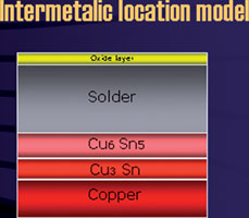
The Cu3Sn is called the depletion layer. When only this layer remains, such as after incorrect soldering, de-wetting occurs and this most often results in rejects and scrapped boards.
To know more about this and how to prevent this from happening I suggest we leave it to a later opportunity where I hope to explain the full circle of quality (and training) in electronic assembly.
For more information contact Eddy van den Wijngaerd, +27 (0)21 712 5964, [email protected]


© Technews Publishing (Pty) Ltd | All Rights Reserved
 printer friendly version